Speccing Flash Size on a 32-bit MCU
Speccing the flash on a 32-bit MCU is deciding, before the firmware exists, how much program memory the part will carry for its whole production life. Flash is the costliest memory on the die. The figure cannot be changed once the part is chosen, so the number is a one-way bet placed at the start of the design. Guess high, and every unit ships with silicon it never uses. Guess low, and a late feature meets a wall. The skill is estimating the real footprint after growth and buying the smallest part that holds it, in a family that leaves a way up.
The costliest memory on the die
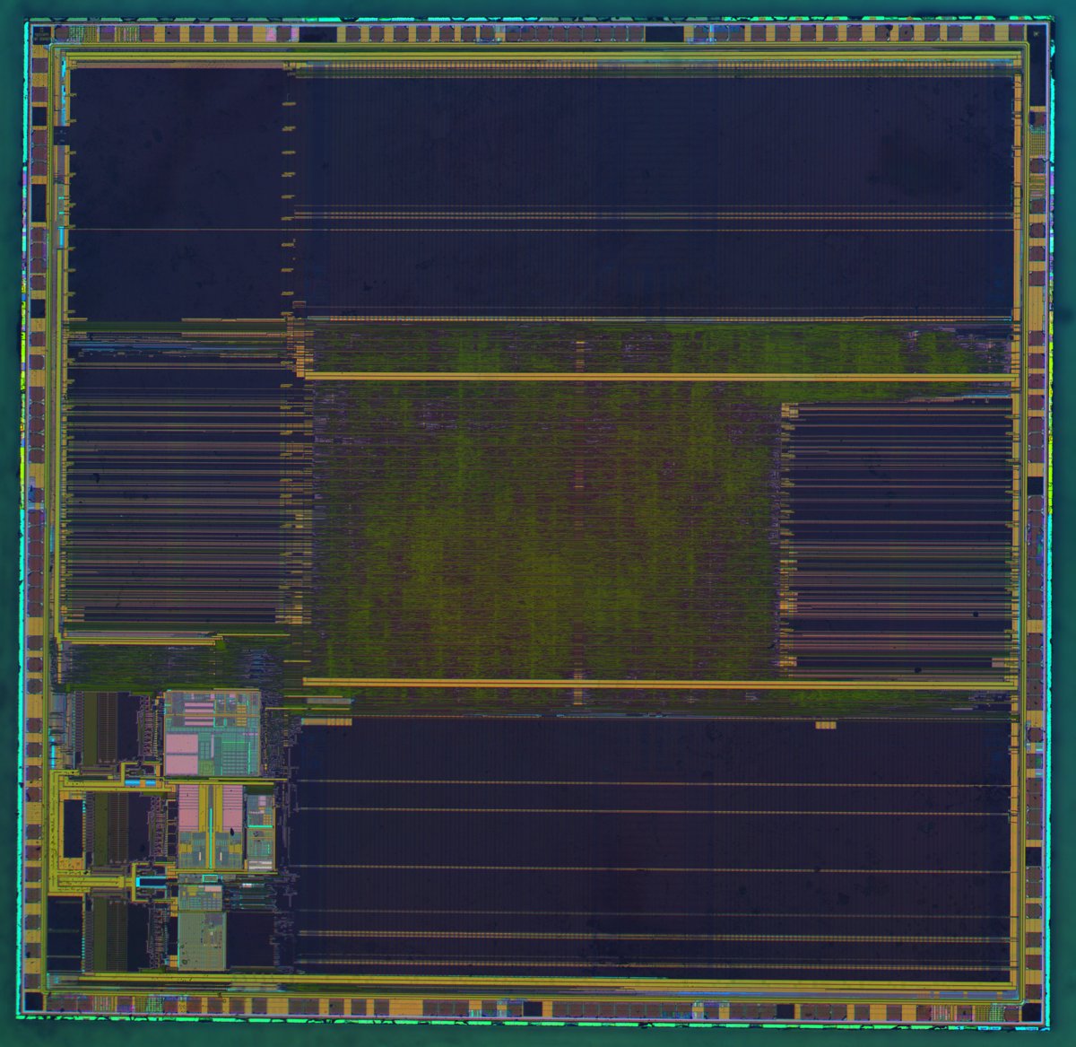
Flash is the costliest memory a microcontroller carries. It moves the part price more than any other line item. On the die, the flash array is a large block of regular cells that takes up a big share of the silicon, far more area than the processor core that runs the code. Pay for a megabyte of flash, and the bulk of what is bought is that array. A part number a design commits to is, in cost terms, a flash size with a core attached to it.
Embedded flash is dear for a physical reason. The floating-gate cells that hold a charge for years are not built in the same process as the logic around them; they need extra mask layers and extra steps on every wafer. A larger array costs more silicon to make and more to test. That cost runs straight through to the part price. The processor core, the RAM, and the peripherals together can take less die area than the flash on a part that carries a megabyte of it. Read down the price list of a single MCU family. Each step up in price buys more flash and almost nothing else. Speccing flash is, in plain terms, speccing the largest cost driver in the part.
The number specified at design time is fixed for the life of the part. It cannot be added later by a software change or a board rework. A part with 256 kB has 256 kB until the design moves to a different part number. That immovability is what makes the figure deserve more thought than the clock speed or the peripheral list, both of which a design can usually work around. Flash is special silicon for a reason beyond cost. It holds its contents for years with the power off and survives a rated number of erase cycles. Those are the properties the extra process steps buy. The design pays for that permanence in die area and in price when it chooses the part number.
So a 32-bit MCU is chosen, in large part, by how much flash it carries. The figure sits among the first decisions a design commits to. It is also among the hardest to take back, since taking it back means choosing a new chip. A clear estimate at the start is cheaper than a part change at the end.
What fills it
The application’s own code is almost always the smallest part of the total. What counts as the application is the business logic the product was built to run: the control loop, the state machine, the handful of algorithms that make it the thing it is. That logic is rarely the part that fills the flash. A vendor’s hardware abstraction layer, linked in for convenience, can outweigh the application logic it wraps. An RTOS kernel adds a few kilobytes more. The plumbing around the logic, the drivers, the stacks, the libraries, and the runtime, is what a budget keeps underestimating.
Connectivity is the heavyweight, because a radio stack is a large body of tested, certified code that ships as one block. A Bluetooth Low Energy stack is the clear example: Nordic’s S140 SoftDevice occupies around 148 kB of flash before the application adds a single line. A TCP/IP stack, a USB device stack, a TLS library with its certificates, a Wi-Fi or Thread or Matter stack each land somewhere from tens into hundreds of kilobytes. A connected product often carries several of them at once. A design that sizes its flash for the application alone has undersized the part before a feature is written, because the stack the radio needs was never in the budget. The stack also comes in layers a budget has to count in full. A wireless solution carries a link-layer controller, a host with its protocol layers, and the profiles or services on top. A security layer pairs and encrypts the link. A vendor may ship all of this as one pre-qualified binary, or as source the build compiles in. Either form takes the same room. On a wireless product the stack is often the largest single tenant of the flash. The flash plan starts from it and adds the product on top.
The toolchain adds weight before the application does. A full C library brings formatted printing, floating-point conversion, and locale handling into the image. A single printf that formats a float can pull in tens of kilobytes of library code on its own, which is why vendors ship cut-down libraries for parts where the space is tight. The same source compiles to different sizes depending on whether the build is tuned for size or for speed. A size-optimised release build can be a fraction of the debug build it grew from. All of it sits in flash before the application logic adds a byte. It is the cost of the tools and the language the code is written in.
Graphics and stored data can dwarf the code outright. A user interface on a colour display pulls in fonts, icons, and bitmaps. Those assets run from tens of kilobytes into the hundreds. A single screen of artwork can take more flash than all the application code. Audio prompts, look-up tables, and machine-learning model weights live in the same flash, each sized in its own right. A graphics framework adds its own code on top of the assets it draws. A high-colour image compresses only so far before it loses the look the product was sold on. The assets tend to grow over a product’s life when screens are added or redesigned, which makes them one of the reservations a design has to size for where the product is heading.
Two more tenants are easy to forget. The bootloader takes its cut, a small block that has to be there before any of the application runs. Non-volatile storage takes another, whatever the product reserves in flash for an emulated EEPROM, a calibration record, or a log, sized for the largest amount it will ever hold. That reserved space is flash the code never gets to use.
Two ways to be wrong
Flash size punishes a wrong guess in both directions, which is what makes it hard. Guess high, and unused silicon ships on every unit and keeps costing for the life of the product. Guess low, and a late feature or a security patch one day will not fit; the fix is a new part, a new board, and a new round of qualification. The number has to be settled early, because changing it after the first shipment means changing the chip the product is built on. The wall does not announce itself in advance. It stays invisible until the day a build will not link or an update will not fit. By then the part is on a thousand boards, and the only fix is a full re-spin.
The room you leave empty
Even a perfect estimate of today’s firmware is the wrong number to specify, because the part has to hold more than today’s firmware. The largest reservation is usually the update. A product that takes firmware over the air needs a place to put the new image while the running one keeps the device alive. The robust way to do that holds two full application slots in flash at once, an A slot and a B slot. The device runs from the valid slot and downloads into the other, then boots the new one and keeps the old as a fallback. That design survives a power cut in the middle of a download, since the running image is never the one being overwritten. It costs what it sounds like it costs: the code reservation doubles. A small metadata region records which slot is valid and how many times each has booted, so the bootloader can roll back to the last good image after a failed update. On some parts the two slots map to two physical flash banks the hardware reads and writes at the same time, so the device keeps executing from the active bank while the spare bank is erased and reprogrammed in the background, with no halt in the running code. The slots have to align to the sectors the flash erases in, which rounds each slot up to a sector boundary and reserves a little more than the image itself. A signed image carries its signature and a header the bootloader checks before it hands over control, a few more bytes on top of the code. A design that cannot spare the double can use a single staging slot and swap in place, accepting a riskier update, or compress the image and trade flash for the time and code to decompress it. The dual-slot layout is the one a connected product usually settles on, because a bricked unit in the field costs more than the flash that would have prevented it.
The update is the big reservation. Others sit beside it. The bootloader that manages the swap is a small block that has to be there before anything else runs. A secure boot adds the verification code and the public keys it checks images against, more flash spent on trusting what runs. Non-volatile storage takes its own region, whatever the product keeps in flash for calibration, settings, or a log, sized for the largest amount it will ever hold and often wear-levelled across extra spare pages. Flash wears a little on each erase, rated for a fixed number of cycles, so a region written often needs extra pages to spread the wear and a small file system to manage them, both of which add to the reserved size. Manufacturing leaves its own marks as well, a serial number, a MAC address, a per-unit calibration table, each in a page set aside for it. A few pages hold the option bytes and the protection settings the part boots from. Each of these regions has to start on a sector boundary, since the flash erases a whole sector at a time, so the reserved size rounds up to whole sectors. Development and debug builds compile larger than the size-optimised release, because the compiler keeps the code easy to step through, so the part has to hold the bigger of the two through the whole project. A recovery path adds more still. A product that can be restored after a bad update keeps a factory or golden image in a protected region of flash, a third copy beside the two update slots, sized like the application it restores. The designs that carry it accept the extra flash as the price of always being able to bring a unit back. And the future has to fit: the feature added in year two, the protocol a customer asks for, the security fix that grows the stack after launch. Each of these reservations is small next to the update. Together they still add up to real flash a budget has to count. The working number is today’s honest footprint, the update reservation on top, the bootloader and the storage beside it, and a real margin for the years the product will live.
Buying margin by the rung
The cheapest insurance against a low guess is a part that swaps for a bigger one on the same board. Vendors sell a flash range across one footprint: the STM32F103 in an LQFP64 package runs from 64 kB on one part number through 128, 256, 384, and up to 512 kB, each pin-for-pin identical. A design lays out for the middle of that range, fits the firmware to a lower rung, and keeps the higher rungs in reserve. If the code outgrows the chosen part, the next number up drops into the same footprint on the same board. Flash and RAM usually climb the ladder together, so the step that buys more code space buys more working memory beside it. The range can be wide. A single Cortex-M family often spans from tens of kilobytes at the bottom to a megabyte or two at the top, the same core and peripherals throughout, the flash and the price the main things that move along it. A design that knows roughly where its firmware will land picks a part a rung or two below the ceiling, so a way up is always there. The gap between two rungs is often a matter of cents at volume, which is what makes a deliberate step up so much cheaper than a redesign.
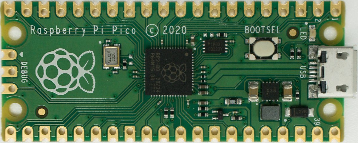
When the assets outgrow any on-chip flash, the flash moves off the chip. A serial flash chip on a QSPI or OSPI bus adds megabytes for graphics, audio, or model weights. The processor can execute code from it in place, so external flash extends the program space as well as the data space. Some parts take this all the way. The Raspberry Pi RP2040 runs entirely from up to 16 MB of external QSPI flash. The chip holds none of its own. The decision then has two parts: how much fast on-chip flash the core needs for its hot code, and how much bulk flash the assets need beside it. External flash is not a free extension of the internal kind. The QSPI bus runs slower than the internal flash bus, so code executed in place from it runs behind code in on-chip flash. A cache between the two hides the gap only for code that stays hot. The chip adds its own cost, its own board space, and a handful of pins to route. Only the timing-critical code and the interrupt handlers need to live in the fast internal flash. Sizing then becomes two numbers, an internal figure for the code that has to be quick and an external figure for the bulk that only has to be present. Some parts soften the pin and board cost by stacking the QSPI flash in the same package as the processor, a system-in-package that looks like one chip and still lets the design pick the flash density at order time. Even a part with no internal flash needs a little fast memory to start from, a boot ROM or a small internal block that brings the external bus up, since the core has to run before the QSPI device answers.
The ladder is a planning tool as much as a parts list. A team that picks the family early, lays the board out for a mid-range footprint, and tracks the firmware size against the chosen rung through development can see a low guess coming and step up before the board is fixed. The step that stays inside one family costs only the price difference between two part numbers, because the board, the firmware, and the qualification all carry over unchanged. That is the cheapest kind of margin a design can buy. It is why a family with a long flash ladder earns its place even when today’s firmware fits the smallest rung.
Picking the number
The method is an honest estimate, run early. The linker’s map file is the real measurement: it reports the exact size of every section once the firmware builds. Watching that number through development catches growth while there is still room to act. Add up the real footprint: the application, the libraries and stacks it links, the assets it carries, the bootloader, and the storage it reserves. Double the code portion if the product updates over the air. Add a margin for the years the product will live. That total points at a flash size.
A worked estimate shows the shape of it. A connected sensor might run forty kilobytes of application logic, thirty of vendor HAL, a hundred and fifty for the BLE stack, a hundred for its display assets, and twenty reserved for storage. That sums to around three hundred and forty kilobytes before any margin. A safe over-the-air update doubles the application side. The total then runs past five hundred kilobytes. The smallest standard rung above that is a megabyte, so the honest answer for a product that looked like a quarter-megabyte job is a one-megabyte part. A team that had specced for the application alone would have ordered 256 kB and hit the wall during the first firmware update. The number that comes out of an estimate like that is rarely the number a first guess would have reached. That gap, found on paper, is the whole reason to run the estimate while the part can still be changed.
Round up to the next rung the vendor sells, and favour a part in a family where the rungs above it share the footprint. A design that lands on the smallest part holding the honest total, with a steppable path above it, has spent the least silicon the job allows and kept a way out if the guess ran low. A rule of thumb fills the chosen part to something like half or two-thirds of its capacity on launch day, which keeps the rest for the update slot, the storage, and the years of growth. Filling a part to the brim on day one is the same mistake as undersizing it, with the wall only a little further off. One last check belongs on the chosen rung: that the part is stocked and second-sourced at that flash size, since a number that lands on a part nobody can supply is its own kind of wrong. The figure that survives all of this is rarely round, and rarely the one the first guess reached for.
Size for what the firmware will become. The first day is the smallest it will ever be.
That is the whole discipline: size for what the firmware will grow into, and buy the room to grow in the cheapest form there is, a higher number on the same footprint. The part that fits the honest total is the one a design lives with for the product’s whole life, provided the family it belongs to can climb.
| Component | Typical flash | Note |
|---|---|---|
| Application logic, small product | 10 to 50 kB | the part an estimate starts and stops at |
| Vendor HAL / driver layer | tens of kB | can exceed the application it wraps |
| RTOS kernel (FreeRTOS) | a few to ~10 kB | small on its own |
| BLE stack (Nordic S140) | ~148 kB | before the application adds a line |
| TLS library and certificates | tens of kB | crypto code plus keys |
| One GUI font, usable size | tens of kB | per typeface |
| Screen of artwork or bitmaps | hundreds of kB | per screen |
| Dual-image OTA reservation | 2x the code size | two full images held at once |
How much flash headroom should I leave?
Enough for the update mechanism, the bootloader, the reserved storage, the larger debug build, and the growth the product will see over its life. A dual-image over-the-air update alone roughly doubles the code reservation. A common result is a specified size well above the footprint of the firmware on launch day.
Does a Bluetooth or Wi-Fi stack really need that much flash?
Yes. A Bluetooth Low Energy stack like Nordic’s S140 SoftDevice takes around 148 kB before the application adds anything. A TCP/IP stack, a USB stack, a TLS library, and a Wi-Fi, Thread, or Matter stack each run from tens into hundreds of kilobytes. A connected product frequently carries several of them together.
What happens if I undersize the flash?
A late feature or a security patch eventually will not fit. The fix is a part change: usually a new footprint, a board re-spin, and re-qualification. That is the expensive failure mode, which is why a design leaves headroom and favours a family it can step up within.
Is it bad to oversize the flash?
Oversized flash is die area the product pays for on every unit it ships, plus extra programming and erase time per unit on the line. The aim is the smallest part that still holds the footprint after honest growth.
Can I add flash externally instead of speccing a bigger MCU?
Yes, for bulk assets. A serial flash chip on a QSPI or OSPI bus holds megabytes of graphics, audio, or data. The core can run code from it in place. Some parts, such as the RP2040, run entirely from an external QSPI device sized on its own. They carry no internal flash of their own.