Silicon is the second most abundant element in the crust, locked up almost entirely as oxide. Getting it out means taking the oxygen off, and that reaction needs heat on an industrial scale. Quartzite goes into a submerged arc furnace with a carbon source, usually coal, coke and wood chips. Electrodes carry current down into the charge. Temperatures near them reach around 2,000 degrees. Carbon strips oxygen from silicon dioxide. Molten silicon collects at the bottom while carbon monoxide leaves the top. What tapped out of that furnace is metallurgical grade silicon, about 98 percent pure. That grade is entirely adequate for aluminium alloying and for silicone chemistry, which consume most of world production. Two percent of anything else is catastrophic for a solar cell. Put that in units the industry uses and the gap becomes clear: 2 percent is 20,000 parts per million. Electronic grade material is specified below one part per billion. Bridging that gap means removing impurities by a factor of about twenty million. Every step that follows exists to do it.
Nine nines, by way of a gas
Purification runs through a gas because gases can be distilled and solids cannot. Ground metallurgical silicon meets hydrogen chloride in a fluidised bed reactor. The reaction produces trichlorosilane along with a mixture of related chlorosilanes. Distillation does the actual cleaning. Chlorosilanes boil at different temperatures from the chlorides of the metals contaminating them. Repeated fractional distillation strips iron, aluminium, boron and phosphorus down to trace levels. Nothing about that stage is exotic chemistry. A refinery works on that principle, with a feedstock whose specification is a billion times looser. Repetition is what reaches parts per billion. A single distillation stage separates two liquids by some factor, and putting the product through another stage applies the factor again. Three stages each cutting an impurity a hundredfold leave a millionth of what went in. Columns run continuously with dozens of theoretical plates for exactly that reason. An impossible-sounding specification is an ordinary separation run many times over.
Deposition puts the silicon back into solid form. Purified trichlorosilane and hydrogen flow into a bell jar containing U-shaped silicon seed rods heated to about 1,150 degrees. Silicon comes out of the gas and grows onto the rods. Days of that thickens them into columns of polycrystalline material. The rods get broken up into the grey chunks that arrive at a crystal puller. Conventional Siemens material lands at nine nines of purity, with impurity levels under one part per billion. That number is the reason a solar cell works at all. Every impurity atom is a potential recombination centre. The whole value of a single crystal disappears once the crystal is dirty.
Pulling one crystal from a melt
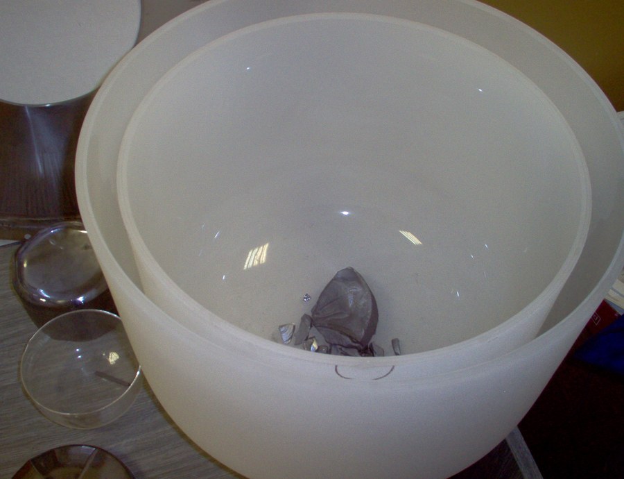
A fused quartz crucible after a pull, with the last of the melt frozen in the bottom. Silicon attacks quartz at 1,414 degrees, so the crucible is consumed by every run and dissolves oxygen into the crystal while it does. Photo public domain.
Polysilicon chunks go into a crucible of fused quartz inside a graphite susceptor. Dopant goes in with them, boron or gallium for p-type material, in quantities measured against a melt of hundreds of kilograms. Heaters bring the charge above the melting point of silicon at 1,414 degrees. Argon fills the furnace at reduced pressure. A seed crystal of known orientation descends until it touches the surface. Surface tension holds the melt against it. The seed then rises, slowly, while seed and crucible rotate in opposite directions. Silicon freezes onto the seed following the lattice orientation it finds there. Argon is doing a job as well. Silicon at 1,414 degrees reacts with anything available. An inert atmosphere at reduced pressure keeps oxygen and nitrogen away from the melt. It also sweeps away silicon monoxide evaporating from the melt surface, which would otherwise condense on cooler parts of the furnace and fall back in as particles. A particle landing on the growth front ends the dislocation-free run instantly. Rotation is not decoration. It stirs the melt, evens the temperature around the growth front, averages out asymmetries in the heater. Pull rate and rotation speed together set the diameter. An operator holds it by adjusting both against a camera watching the meniscus. The crucible pays a price for all of this. Molten silicon attacks fused quartz. Oxygen enters the melt continuously and ends up dissolved in the growing crystal. A quartz crucible survives one pull. Every ingot carries the chemical signature of the vessel it came from. That crucible then goes to scrap. Length is limited by that vessel too. A charge of a few hundred kilograms feeds one pull, and once the melt runs low the growth front sits closer to the crucible wall where the temperature field is worse. Recharging systems drip fresh polysilicon into the melt during growth to stretch a run. One crucible then pays for more metres of crystal.
The thin neck that fixes everything
Touching a cold seed to a melt at 1,414 degrees does violent things to a crystal lattice. Thermal shock generates dislocations at the contact. Those dislocations propagate down the length of the crystal unless something stops them. The standard fix is elegant enough to be worth understanding. After contact the operator pulls fast and hot, narrowing the crystal to a neck of a few millimetres diameter over a length of a few centimetres. Dislocations in silicon glide on planes inclined to the growth direction. In a thin neck they travel sideways and reach the free surface within that short distance. What emerges below the neck is dislocation free. Everything about the method looks alarming. A neck of a few millimetres carries a body weighing over a hundred kilograms by the end of the pull. The whole crystal hangs from it. Puller design has spent decades on that tension.
Research has found ways around it. Heavily boron-doped or germanium-doped seeds suppress dislocation generation through solid solution hardening. Dopant atoms strain the lattice enough to resist dislocation motion at the seed interface. Crystals up to eight inches in diameter have been grown dislocation free with no thin neck at all.
Squaring the cylinder and slicing it
A finished ingot is a cylinder with a domed crown and a tapered tail. Both ends get cut off. The crown solidified before growth stabilised. The tail carries the impurities the growth front rejected all the way down. Squaring comes next. Four flats get ground along the cylinder to produce the pseudo-square section. Corners stay rounded where the original diameter ran out. Everything ground away goes back to the melt for the next pull. Nothing removed at this stage is wasted. Crown, tail, grinding swarf and broken wafers all return to a future melt, since the material is still pure silicon and only its shape is wrong. The energy that went into growing that crystal does not come back with it. Wafering is where the material accounting gets uncomfortable. A diamond-impregnated wire finer than a human hair runs at speed through a web. That web saws hundreds of wafers from one brick at a time. Industrial wafers land around 160 to 180 micrometres thick. Wire diameter sets the floor on that loss. A core wire carrying diamond grit measures tens of micrometres across. The slot it cuts runs wider than the wire by the grit standing proud of it. Thinner wire cuts a narrower slot and snaps more readily under tension. Wire suppliers and wafer makers negotiate that trade continuously.
Work out what the saw eats. A wire producing a 160 micrometre wafer while removing a 60 micrometre kerf converts 60 out of every 220 micrometres of ingot into slurry, which is 27 percent of a crystal that took days to grow. Diamond wire narrowed that slot considerably against the slurry sawing it replaced. Thinner wafers push the ratio the wrong way. Kerf shrinks more slowly than thickness does.
Etching the saw damage into pyramids
A wafer off the saw is mechanically wrecked at the surface. Microcracks run some microns deep on both faces. Any crack is a recombination site sitting exactly where light is absorbed. Alkaline etching removes that layer and produces something better while doing it. Silicon in a hot sodium hydroxide bath etches at different rates on different crystal planes. The slowest planes survive as facets.
On a single crystal cut along its usual orientation those facets emerge as random pyramids a few microns tall, covering the whole surface. Pyramids earn their place through geometry. Light striking a flat surface reflects once and leaves. Light striking a pyramid face reflects toward a neighbouring pyramid. The wafer gets a second chance to absorb it. Reflection falls substantially before any coating goes on.
Pyramid height has an upper limit set by what comes next. Facets a few micrometres tall trap light well and still accept a uniform coating. Push the texture taller and the deposited nitride thins on the peaks. Printed paste then bridges the valleys in place of filling them. The cell loses more at the contacts than the texture gained in absorption. Etch time and bath chemistry are set against that ceiling. A second benefit shows up later in the line. Screen-printed paste fills the pyramidal texture better than it wets a flat surface. Contact between metal and silicon improves, which lowers series resistance in the finished cell. Texturing is one of the few steps that pays twice.
Building the junction in a furnace
Doped silicon on its own is not a solar cell. A cell needs a junction between p-type and n-type material. Industry builds one by driving phosphorus into the surface of a boron-doped wafer. Wafers enter a quartz tube furnace at 800 to 900 degrees, where phosphoryl chloride vapour and oxygen react at the surface to deposit a phosphosilicate glass. That glass is the dopant source. Phosphorus diffuses out of it into the silicon during the deposition, then further during a drive-in step with the gas supply shut off. Depth and concentration are the whole game. Too shallow and the metal contacts punch through the layer. Too deep or too heavily doped and recombination in the emitter eats the blue response of the cell. Furnace time and temperature set the profile. Process engineers spend careers on that trade. Sheet resistance is the number a process engineer actually watches. It describes the emitter as ohms per square, measured by a four-point probe on a test wafer from each run. Depth and doping arrive as one figure in seconds. A furnace drifting warm shows up as sheet resistance falling before any cell has been finished. That is why the measurement sits at the furnace exit. Uniformity across the wafer matters as much as the average. A furnace loads dozens of wafers in a boat. Gas has to reach every surface at one rate. Gas flow, boat spacing and tube geometry all end up in the recipe. Wafers at the ends of a boat see conditions the ones in the middle do not, which is why boats get loaded to a pattern and the end slots sometimes stay empty. Cleanup follows. The phosphosilicate glass gets etched off in hydrofluoric acid. The junction has also formed around the wafer edges, shorting front to back. An edge isolation step removes it with a laser or a plasma. A cell that skips edge isolation has a permanent shunt across its junction. One layer goes on after the junction and does three jobs at once. Plasma-enhanced deposition lays down silicon nitride, which cuts reflection, passivates the front surface by tying off dangling bonds, and carries hydrogen inside the film itself. That hydrogen is the third job. It waits for the firing step. Heating the cell drives hydrogen out of the nitride in atomic form. Some of it diffuses into the silicon underneath, attaches to defects in the bulk and quietens them. A layer deposited for optical reasons ends up improving carrier lifetime deep inside the wafer. Film composition and density control how much hydrogen is available. Nitride recipes get tuned against lifetime measurements, with colour only a first check.
Printing the metal on
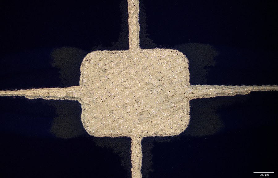
A screen-printed pad where two fingers cross, seen under a microscope. The granular texture is sintered silver particles left after the organic binder burned away. The scale bar at lower right marks 200 micrometres. Photo by Radiotrefoil, CC BY-SA 4.0.
Current has to leave the cell somehow. The contact grid is where optical and electrical demands collide. Every strip of metal on the front face collects current from the silicon under it. It also blocks light from reaching that silicon. Screen printing puts the pattern down. A stainless mesh screen, typically 200 to 325 threads per inch, carries the emulsion pattern of fingers and busbars. Silver paste gets forced through the open areas onto the wafer. A low temperature dry near 120 degrees drives off solvent before anything else happens.
Firing turns printed paste into a contact. Cells pass through an infrared belt furnace between roughly 700 and 1,000 degrees for a minute or two. Organic binders burn away. Glass frit in the paste eats through the anti-reflective nitride layer underneath. Silver reaches the silicon and forms an ohmic contact, a trick the industry calls fire-through. Rear aluminium paste alloys with the silicon during that pass. Colour is a free process check at this stage. Nitride thickness sets the interference condition. The film reflects whatever wavelength it fails to cancel. A correctly deposited layer reads dark blue to the eye. A batch coming out purple or gold has been deposited too thick or too thin. An operator sees that across a room before any instrument gets consulted. Every dimension in that grid is a compromise.
Wider fingers carry current with less resistance. They also shade more silicon. Narrower fingers shade less and lose more to resistance. Taller printing helps both at once, which is why fine-line printing and multi-busbar layouts have absorbed so much development effort. Current mainstream cells add two steps at the rear that a basic line does without. A dielectric stack goes onto the back surface to passivate it. An unpassivated rear recombines carriers that reached it.
That stack also blocks electrical contact. A laser opens fine lines through it before the aluminium paste goes on, leaving contact only where the pattern allows. Both steps exist to raise one quantity: how long a carrier survives before recombining. A rear that reflects light back into the cell adds a second gain. Long-wavelength photons that reached the back get another pass through the silicon.
Testing, sorting and what the yield costs
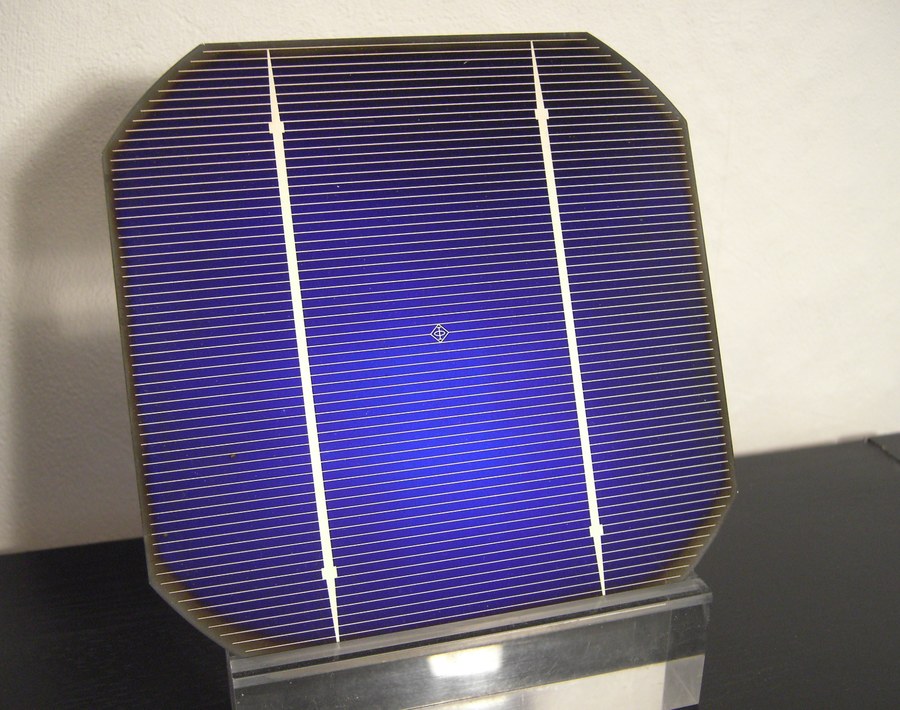
A finished pseudo-square cell. Dozens of fine fingers collect current across the surface and hand it to two wider busbars, and the chamfered corners record the round ingot the wafer was cut from. Photo by Stephan Kambor, CC BY-SA 2.5.
Finished cells go under a flash tester. A xenon lamp delivers a calibrated pulse approximating the standard spectrum. The tester sweeps the current-voltage curve during that flash. Out come the numbers a datasheet is built from. Flash duration matters more than it sounds. The pulse lasts milliseconds, short enough that the cell has no time to warm, which keeps the measurement at the 25 degrees the standard demands. A steady lamp would heat the cell during the sweep and report a figure several percent low. Sorting follows immediately. Cells that fail outright get pulled here as well. A cracked or shunted cell caught at this station costs one cell. The identical fault reaching a finished module costs the module. Bins are narrow, often a few watts wide at module scale. A factory running one product line accumulates bins it cannot use until enough cells arrive to fill a batch. Cells get binned by power output. A module gets built from one bin, never from a mixed batch. That practice traces back to one fact about a series string. A string delivers what its weakest member allows. Mixing a strong cell with a weak one wastes the strong one on every cycle.
The route from quartzite to a finished cell, with the numbers each stage works to
Stage
Conditions
What comes out
Carbothermic reduction
arc furnace, about 2,000 °C at the electrodes
metallurgical silicon, about 98 percent pure
Chlorosilane route
fluidised bed with hydrogen chloride, then distillation
purified trichlorosilane
Siemens deposition
seed rods at about 1,150 °C
polysilicon at 9N to 11N, under 1 ppb impurity
Czochralski pull
melt at 1,414 °C, argon, counter-rotation
one continuous crystal, dislocation free
Squaring and wafering
diamond wire, roughly 60 µm kerf
wafers 160 to 180 µm thick
Texture etch
hot alkaline bath
random pyramids a few µm tall
Emitter diffusion
quartz tube at 800 to 900 °C with POCl₃
n-type layer and a phosphosilicate glass
Screen printing
200 to 325 mesh screen, dried near 120 °C
silver fingers and busbars
Co-firing
belt furnace, 700 to 1,000 °C, one to two minutes
fired-through ohmic contacts
Flash test
xenon pulse at the standard spectrum
cells sorted into power bins
Cost sits mostly upstream of the cell line. Anyone comparing two cell prices is mostly comparing two wafer prices with a thin layer of processing on top. Polysilicon, crystal growth and wafering carry the energy-intensive steps and the expensive consumables, which puts the majority of a finished cell’s cost behind it before the first etch bath. Cell processing adds silver, chemicals and furnace time. That distribution explains a two-decade chase after wafer thickness and kerf. A percent saved on silicon outweighs a percent saved almost anywhere else. Yield compounds in a way that punishes long lines. Run ten sequential steps at 99.5 percent each and the survivors come to 0.995 raised to the tenth, which is 95.1 percent. Drop each step to 99 percent and the line delivers 90.4. Half a percent per step decides whether a factory keeps five wafers in a hundred or ten. Handling has been automated for exactly that reason. Line speed compounds the pressure, since a modern cell line processes thousands of wafers an hour and a jam that breaks one wafer can break the ones behind it. Wafers move in cassettes and transfer on belts and vacuum pickups. Human hands touch them as little as the process allows.
Breakage haunts the whole line. A 160 micrometre wafer is a sheet of brittle crystal the size of a dinner plate. Every transfer, bath and print is a chance to crack one. Thinner wafers save silicon and break more often. Yield is the constraint keeping thickness where it is. Count the thermal excursions a wafer survives and the achievement looks larger. Melting at 1,414 degrees, diffusion near 900, firing near 800, with etches and rinses between them. Each high-temperature step is a chance for impurities to move where they are not wanted. The purity spend at the front of the line is what makes the rest possible.
Common questions
Why does making solar silicon take so much energy?
Two stages dominate. Carbothermic reduction runs an arc furnace near 2,000 degrees. Siemens deposition holds rods at 1,150 degrees for days. Both are unavoidable given where silicon starts, chemically bound to oxygen in sand.
What is the difference between solar grade and electronic grade silicon?
The difference is in the specification. Electronic grade runs to nine or eleven nines for semiconductor use. Solar tolerates slightly more. A cell cares about carrier lifetime where a transistor cares about yield. Some producers sell a dedicated solar grade at lower cost.
Why are cells still 160 micrometres thick when thinner would use less silicon?
Breakage. A thinner wafer saves material and cracks more readily during handling, printing and stringing. The industry has moved thickness down slowly. Yield holds it back.
Is the silver in a cell recoverable?
In principle, through the recycling chain that processes retired modules. Silver sits as a fired paste bonded through the nitride into the silicon. Recovering it means chemical processing, with mechanical separation no use at all.
Does a longer diffusion make a better cell?
Not past a point. A deeper, heavier emitter is easier to contact and worse at collecting blue light. Carriers generated near the surface recombine in the heavily doped layer before collection. The profile is a compromise set in the furnace recipe.