






Comparing the Cortex-M0 M3 and M4 on Performance and Cost
The Cortex-M0+, the Cortex-M3, and the Cortex-M4 are the three Arm cores a general-purpose 32-bit design picks among. They share one instruction base and one toolchain, so the choice between them comes down to two numbers: the work a core finishes per megahertz, and the price of the part that carries it. A core that does more per clock costs more in silicon and in power. The job decides how much of that performance a design uses, and how much it pays for headroom it leaves idle.
Three rungs, one decision
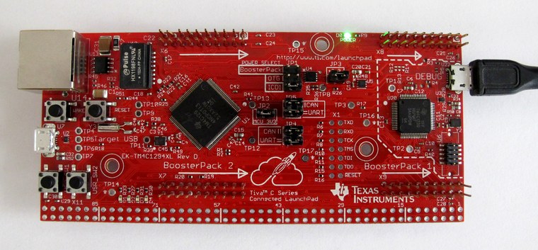
These three cores cover the span a general-purpose microcontroller design works in, from a part that mostly waits on a sensor to one that closes a fast control loop with real math. The same Thumb instruction base runs under all of them, and the same compiler, debugger, and library set serve each one. A team that learns one of the three reads the next from the same mental model. The M3 and the M4 run the full Thumb-2 set, a mix of 16-bit and 32-bit instructions that packs dense code at near-32-bit speed. The M0+ runs a smaller Thumb subset, enough for control and integer work. The interrupt controller, the system timer, and the debug model come from Arm across all three, so a driver written for one moves to another with the register map adjusted underneath. Code density matters in this comparison, since denser code fits more program in the same flash and fetches fewer bytes per instruction. Thumb-2 on the M3 and M4 holds that density high. The Thumb set on the M0+ holds enough code density for the control work an entry part runs. None of the three runs Linux or a rich application stack; that load belongs to a Cortex-A part, a different family with its own page in the wider tree. The three sit close enough that a board can sometimes be laid out to take more than one, with the footprint shared and the part fitted at build time. That option turns the core choice into a late decision, made once the firmware load is measured on the bench. The shared architecture is what makes such a hedge cheap to keep open.
The comparison reads three things against the job. The first is the work a core does per megahertz, the measure of how much each clock buys. The second is the clock ceiling a vendor offers on a part. That ceiling multiplies the per-clock figure into work per second. The third is the cost the part asks, in unit price, in silicon area, and in power. Reading all three lands a design on the core that fits the work at the lowest cost it can. The numbers interact in ways a single figure hides. The slower core per clock can still finish a job on time at a higher clock. Hardware math finishes in a few cycles what a smaller core grinds through in software. The point of the read is the work the product does, measured against the part that does it for the least. A clean way to run it sets the performance need first, draws the line of cores that clear it, then sorts that short line on price and power. The order keeps cost from pulling a design onto a core that cannot do the work, since the performance gate comes before the price sort.
What each core does per megahertz
The Cortex-M0+ runs about 0.95 DMIPS per megahertz through a two-stage pipeline. Its instruction set is the integer Thumb core, kept small. Single-cycle access to the general-purpose I/O lets it toggle a pin or read a port in one clock. The small gate count gives it the lowest power and the lowest die cost of the three. The two-stage pipeline keeps the branch penalty low, so the core wastes few cycles on the jumps a control program is full of. Its interrupt entry takes a fixed, short number of cycles, the trait a real-time loop leans on for a predictable response. A control loop, a sensor poll, or a state machine fits inside it with clock to spare. The math it lacks in hardware, such as divide, runs as a software routine. That trade keeps the die small and the current low. The instruction set still covers the multiply and the load-store and branch logic a control program leans on, so the gap shows up only on the heavier math a simple product rarely runs. Memory tops out lower on these parts as well, with flash and RAM kept modest to match the entry role. Vendors clock the M0+ families gently, in keeping with the low-power aim. The whole package, from the short pipeline to the small memory, points at a job that wakes, does a little, and sleeps. Cost-sensitive products in high volume lean hardest on this core, since a few cents saved across a million units is real money. Wearables, remote sensors, and simple appliances live here, where the work is light and the power budget is tight.
The Cortex-M3 runs about 1.25 DMIPS per megahertz through a three-stage pipeline. It carries a hardware divide, the full Thumb-2 instruction set, and bit-band access that flips a single bit in one operation. Its interrupt controller holds more priority levels, with a memory protection unit available as an option. Branch speculation and a longer pipeline let it sustain a higher instruction rate on the mixed code a general program runs. The Harvard-style buses fetch an instruction and touch data in the same cycle. This logic lifts the per-clock figure. It raises the gate count too. The hardware divide finishes in a handful of cycles, the kind of operation an entry core leans on a software routine for. Bit-banding maps each bit of a peripheral register to its own address, so a single store sets or clears a flag in one operation. The bit-band trick saves the read and the write a flag update would otherwise take, a small win that adds up in a tight interrupt routine. The memory protection unit fences a task’s memory off, the foundation a small operating system uses to keep a fault in one task from corrupting another. A design that juggles several peripherals, a small operating system, or a communication stack settles on this rung for that headroom.
The Cortex-M4 matches the M3 on integer work, near 1.25 DMIPS per megahertz, on the same three-stage pipeline. On top of that it carries the DSP instruction set and an optional floating-point unit. Arm documents these as running signal processing operations directly on the Cortex-M4, with a tenfold speed-up on single-precision floating-point math. A single-cycle multiply-accumulate, saturating arithmetic, and SIMD operations turn a filter or a transform from a long software routine into a few cycles. The multiply-accumulate is the inner step of every digital filter. The M4 runs it in one clock. Saturating arithmetic clamps a result at its limit, the behaviour audio and control code needs to avoid a wraparound glitch. The floating-point unit handles single-precision math in hardware, the depth and use of which the FPU guide takes up on its own. SIMD packs two 16-bit or four 8-bit values into one 32-bit register and works on them together, the trick that speeds a pixel loop or an audio frame. The DSP set as a whole is the subject of its own guide, so the point here is simpler: the M4 carries this math on the same core that runs the control code, with no second chip in the path. A product that runs audio, motor control, or sensor fusion reaches this rung for that math.
Performance per clock is half the story. The clock ceiling a vendor offers is the other half. That ceiling runs across the tiers, from a modest figure on a low-power M0+ part to a high one on an M4 family. The top clock multiplies the per-megahertz number into the work the part finishes in a second, so a fast M3 can out-run a slow M4 on plain integer code. The process node, the flash speed, and the power target of the family set that ceiling. Top clocks run from a few tens of megahertz on a low-power M0+ family up to several hundred on an M4 family aimed at compute. The datasheet clock figure sets the upper bound on throughput, a number to read alongside the core name.
The honest measure of a core is the work it finishes per second on the real code. A benchmark close to the product gives that figure, since a synthetic loop can flatter one core or another. The per-megahertz number and the clock ceiling together set the ceiling on that work. The job’s real demand sits somewhere below it, and the distance between the two is the headroom a design pays for. CoreMark and Dhrystone give the rough per-clock figures, useful for a first sort of the three. The figure that decides a design is the one taken on its own workload: the filter, the protocol stack, the control law it runs in the field. A core that wins a synthetic benchmark can still fall behind on the code the product ships, so the bench gets built close to the real thing. Memory speed enters the figure too, since slow flash forces wait states on a fast core. A vendor adds a cache or an accelerator to hide that gap, so the throughput on a real part reflects the memory system as much as the core. The number that counts comes off the candidate part running the product’s own loop.
The cost that rides in the core
The core itself is a small slice of the die. An M0+ core spends a fraction of the gate count of an M3. The M4 adds its math units on top of the M3 logic. On a finished MCU, the flash, the RAM, and the analog usually take more silicon than the core, so the core sets a floor on cost and power. Process node shifts the picture again, since a part built on a denser node packs the same core into less area for less money. A modern M3 or M4 on a fine node can undercut an older M0+ part on an aging one, the cost inversion that shows up across vendor catalogues. The gate count sets the relative order of the cores; the process and the volume set what a buyer pays in the end. The lesson for a buyer is to compare real part numbers on a live quote, since the core name alone gives only the rough tier. Two quotes on the same core, from two vendors at two volumes, can land a long way apart. The vendor’s wrapper around it sets everything above that floor, which is why two parts on the same core can sit far apart on price. Flash, a bank of analog converters, a USB controller, or a radio costs more area than the processor in the middle. The core decides what the part can compute. The price tag answers more to the memory and the peripherals the vendor wrapped around it, and to the volume the part ships in. High volume drives the unit price down through the fab, which is why a popular M3 part can undercut a niche M0+ one on a purchase order. The core comparison sets the performance and power envelope; the actual quote comes from the part number, the package, the temperature grade, and the quantity. A sound read holds the two apart: pick the core class on the work, then shop the specific part on the bill.
Cost past the unit price
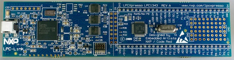
Cost runs past the unit price into the bill of materials. An M4 with its DSP and floating-point unit can absorb a signal-processing job in software. That takes a separate DSP chip off the board, along with its cost, its board space, and its supply line. The math a core does in hardware is the math the rest of the bill does not have to buy elsewhere. An integrated part also saves the board space, the routing, and the second power rail a separate processor would ask for, savings that show up in a smaller, cheaper board. The same logic runs the other way at the low end. Work with no signal math gains nothing from the M4’s units. Reaching past the M0+ there spends silicon the job leaves dark. The cost-aware read counts the whole bill, the core plus the parts a stronger core lets a design delete, against the parts a weaker core forces a design to add.
Power is a running cost on a battery product. A smaller core draws less current at the same clock. It idles at a lower floor too. A coin-cell sensor reaches for the M0+, since its years of life ride on the sleep current. A higher clock and a bigger gate count both raise the active current, so a core that finishes its work fast and sleeps gives back more than one that runs slow and stays awake. Wall-powered designs weigh power far less, where the heat and the regulator size matter more than the milliamps. The power a core saves gets paid back on every day a battery product runs.
Development cost stays flat across the three. One Arm toolchain, one debugger, and one set of CMSIS libraries cover all of them, so a team carries its skills from one rung to the next. Moving a design up the ladder is a recompile, with the peripheral code checked against the new part. The shared platform holds the cost of changing a core down to engineering time alone. The CMSIS layer abstracts the core registers, so the same startup and interrupt code carries across the three. The CMSIS-DSP library ships filters and transforms tuned to the M4’s instructions, ready for a team to call without hand-written assembly. The same code base compiled for an M0+ falls back to the software versions of that math, so a prototype can run on one rung and ship on another. Keeping the math behind the library call leaves the rung an open choice deep into the schedule. Second-sourcing on the same core, from a different vendor, becomes a recompile against its peripherals, the resilience a long-lived product builds in early.
Matching the job to the rung
The match runs from the job to the rung. If the work is a control loop, a sensor read, or a state machine, the M0+ does it at the lowest cost and power. If the work adds several peripherals, a small operating system, or a protocol stack, the M3 carries the headroom for it. If the work runs signal math, audio, or a tight control law, the M4 and its math units earn their price. Each rule names the lowest rung that clears its own job. The rules overlap in a wide middle band, where an M3 and an M4 both clear the work and the choice comes down to the math and the price. In that band, the read is whether the job has signal math that earns the M4’s units. With that math present, the M4 pays for itself. Without it, the M3 holds the same integer speed for less. The lower band splits the same way between the M0+ and the M3, on whether the firmware needs the M3’s headroom, its peripherals, or its memory protection. Naming the heaviest thing the firmware has to do points at the rung every time, since each core’s defining feature answers a specific kind of load. The heaviest task on a thermostat is a slow sensor read, so it lands low. The heaviest task on a motor drive is a fast math loop, so it lands on the M4. Working from the peak load down keeps a design off a core that the worst spike overruns. The peak sets the floor on the core, since the worst spike has to fit inside the cycles the part offers.
Four products show the rule in use. A thermostat that reads a sensor and drives a relay takes an M0+. A handheld meter with a display and a USB link takes an M3. A drone’s motor controller running fast current loops takes an M4. A battery gas-gauge that has to last years takes an M0+ for its sleep current. The job picks the rung. Habit plays no part. The thermostat spends its life waiting between slow events, so the M0+ power floor decides it. The meter drives a screen and talks over USB, the kind of load the M3’s headroom and peripheral count handle. The drone closes a current loop thousands of times a second with real math in the path, the work the M4’s units exist for. The gas-gauge lives on its sleep current, back to the M0+ for the same reason as the thermostat. Each product names its heaviest task. That task lands it on a rung on its own. The pattern holds across the catalogue: the work decides, the core follows, the part number comes last.
Cost-per-job is the read that ties performance and price together. The right part is the cheapest one that finishes the work on time, with a step of margin on top. Go under that and the loop time slips, forcing a late and costly move up a tier. Go over it and the product pays for compute it never runs and power it never needs. The margin guards against the firmware growing over the product’s life, since a part chosen at the exact ceiling of today’s need runs short once features land. The right reserve is one step up, enough room for growth, short of paying for a whole tier the work will never reach.
The three cores are one family read on two numbers: the work a part does per clock and per second, and the cost it asks in silicon and power. Reading its own job honestly lands a design on the rung that does the work for the least, and leaves the headroom it does not need on the shelf. The three cores cover the bulk of the 32-bit control market between them, so the answer for nearly any general-purpose product is one of them, fixed once the work is named in plain terms.
| Core | DMIPS/MHz | CoreMark/MHz | Pipeline | What it adds | Relative cost |
|---|---|---|---|---|---|
| Cortex-M0+ | ~0.95 | ~2.4 | 2-stage | integer Thumb, single-cycle I/O | lowest |
| Cortex-M3 | ~1.25 | ~3.3 | 3-stage | hardware divide, full Thumb-2, bit-band | middle |
| Cortex-M4 | ~1.25 | ~3.4 | 3-stage | DSP set, optional FPU | highest of the three |
Is the Cortex-M4 faster than the Cortex-M3 on ordinary code?
On plain integer code the two run at about the same rate, near 1.25 DMIPS per megahertz on the same pipeline. The M4 pulls ahead only on the math its DSP and floating-point units handle, where a hardware multiply-accumulate or a floating-point operation replaces a long software routine. A design with no signal math sees little gain from the M4 over the M3.
How much slower is the Cortex-M0+ than the M3?
The Cortex-M0+ does about 0.95 DMIPS per megahertz, roughly three-quarters of what an M3 finishes at the same clock. The gap widens on math the M0+ lacks in hardware, such as divide. A part’s top clock matters as well, since a higher-clocked M0+ part can match a lower-clocked M3 on throughput.
Does a Cortex-M4 cost more than a Cortex-M3?
The M4 core adds its math units on top of the M3 logic, so it carries a little more silicon. On a finished MCU the difference is often small, since the flash, RAM, and peripherals dominate the die. The price gap between two real parts comes mostly from what the vendor pairs with the core. The core itself adds little to the bill.
When does paying for an M4 over an M0+ make sense?
The case for the M4 is signal math the M0+ would run too slowly in software, such as a digital filter, an FFT, or a motor control law. The M4 can also absorb a job that would otherwise need a separate DSP chip. That takes the extra part off the bill. A product with only simple control logic saves money on the M0+.
Can one design move between these cores later?
Code written to the Arm architecture and CMSIS recompiles onto any of the three, since the cores share an instruction base. A smaller core that lacks DSP or floating-point math asks for a rewrite of that math. Keeping the math in CMSIS-DSP form eases that move.