Polished silicon is a mirror. Anyone who has seen a bare wafer knows it. A large mismatch in refractive index between air and the material is the reason. Fresnel gives the size of the problem at normal incidence. Reflectance equals the difference of the two indices divided by their sum, all squared. Air sits at 1.00. Silicon around the middle of the visible band sits near 3.9. Put those in. The difference is 2.9. The sum is 4.9. That ratio squared is 0.350. Thirty-five percent of the light arriving at a bare polished wafer leaves again without ever entering the silicon. Bare silicon carries a surface reflection of over 30 percent by that arithmetic. Silicon sits that high because of what it is. Refractive index measures how strongly a material’s electrons respond to a passing field. A semiconductor with a small bandgap has electrons that respond very readily. Glass manages 1.5 by the opposite route: its electrons are tightly held.
Index also changes with wavelength, which matters later. Silicon runs higher in the blue and lower in the infrared. Reflection to be cancelled is itself a moving target across the spectrum. Any single film is solving a slightly different problem at every wavelength it meets. No amount of work on the cell underneath recovers that third. Carrier lifetime, junction depth, contact design and grid layout all operate on photons that got inside. A third of them never did.
Cancelling one reflection with another
The fix is interference. Arrange a second reflection that arrives out of step with the first. Put a transparent film on the silicon and light now meets two boundaries. Some reflects at the top surface, where air meets film. The rest travels through the film, reflects where film meets silicon, then travels back out. One detail decides whether the argument works at all. A wave reflecting off a denser medium flips its phase by half a cycle. Both boundaries here are steps upward in index, air into film and film into silicon. Both reflections flip. Two identical flips cancel out of the comparison. Path difference is left setting the relative phase alone. Those two returning waves overlap. Make the round trip through the film exactly half a wavelength longer than the direct path. The second wave then comes back with its crests where the first has troughs. The two cancel. A round trip means crossing the film twice. A half-wavelength round trip needs a quarter-wavelength film. Everything about anti-reflective coating design follows from that sentence. Notice what the argument never used: the film’s colour, its hardness, its chemistry. Interference cares about optical thickness and index step, nothing else. That is why one line of reasoning describes an oil slick on a puddle and a coating on a solar cell. Two consequences fall out immediately. Both belong to manufacturing. A film cancelling green light has to be a quarter of a green wavelength thick inside itself, which is a distance of tens of nanometres and a few hundred atoms. Depositing that repeatably across a wafer, batch after batch, is the engineering problem behind a step that sounds like painting.
Wavelength inside the film is what matters. Light slows in a dense medium and its wavelength shortens by the index. Six hundred nanometre light becomes 300 nanometre light inside a film of index 2.0. A quarter of that is the 75 nanometres the arithmetic produced.
The two numbers a coating has to hit
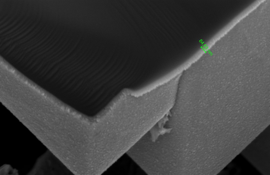
A coated cell surface in cross-section under an electron microscope. The green marker measures the film itself at about 85 nanometres, which is the quarter-wave region this article works through. Photo by Radiotrefoil, CC BY-SA 4.0.
Cancellation needs two conditions met at once. Both come out of that interference argument. Thickness is the first. Optical thickness has to equal a quarter of the design wavelength. Physical thickness equals that wavelength divided by four times the film’s refractive index. Take 600 nanometres as the design wavelength and a film index of 2.0. The thickness works out at 600 divided by 8, which is 75 nanometres. Index is the second. It decides how complete the cancellation is. Two waves only cancel fully when they have equal amplitude.
Amplitude at each boundary depends on the index step there. The film needs to sit at the geometric mean of what lies on either side. Hitting a target index is a deposition question. Plasma deposition builds silicon nitride from silane and ammonia. The ratio between those two gases sets the composition of the film. More silane leaves the film silicon rich and raises its index. More ammonia leaves it nitrogen rich and lowers it. Published work spans indices from about 1.57 to 2.76 on that lever alone. A cell designer needs nothing outside that range.
Run that for a cell in air. The geometric mean of 1.00 and 3.9 is 1.975. Silicon nitride deposited near an index of 2.0 lands within a whisker of the ideal. Residual reflection at the design wavelength falls to about 0.02 percent. Thirty-five percent has become effectively nothing. The film doing it is thinner than a wavelength of the light it cancels. Depositing it costs a few seconds in a tool. Pushing the index higher has a cost that the reflection arithmetic hides. A silicon-rich film absorbs light itself, most of it at the blue end. A photon absorbed inside the coating is lost outright. Reflection at least sends a photon somewhere it might bounce back from. Parasitic absorption ends the story. Film recipes sit where index, absorption and passivation quality are all acceptable, never where any one of them is optimal.
Why the design wavelength is 600 nanometres
A quarter-wave film cancels perfectly at one wavelength. Away from that wavelength the round trip stops being exactly half a wave out of step. Cancellation weakens. Reflection climbs back. Choosing the design wavelength means choosing where to be perfect. The industry settles near 600 nanometres. Two curves multiplied together explain the choice. Solar irradiance peaks in the visible band. Silicon responds across a wide range, weakly at the blue end where photons are absorbed very near the surface and recombine before collection. Response stops entirely past about 1,100 nanometres, where photon energy falls under the bandgap. Multiply the spectrum by that response and the useful power piles up in the middle. Response falls at both ends for different reasons, which is worth separating. Blue photons carry more than enough energy. They are absorbed within the first fraction of a micron, where the emitter is heavily doped and recombination is fast. Infrared photons past 1,100 nanometres carry too little energy to free a carrier at all. Silicon is transparent to them. Neither loss is anything a coating can fix. A film moves photons across the boundary. What happens to them afterwards belongs to the silicon, to the junction depth and to the carrier lifetime underneath.
Six hundred nanometres sits in that pile. A coating tuned there gives up performance in the deep blue and the near infrared, where less was on offer. Its gain lands where photons and response overlap.
Why a finished cell looks blue
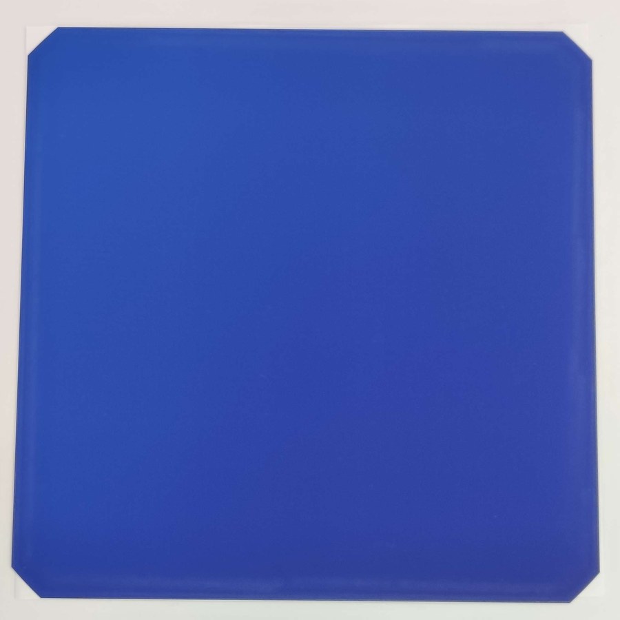
A cell precursor before any metal goes on. Nothing is left on the surface except the coating, so the colour is the coating: the wavelengths it cancels are gone, and what returns to the eye is what it failed to cancel. Photo by Radiotrefoil, CC BY-SA 4.0.
Colour on a coated cell is a direct readout of the design. Wavelengths near the design point are being cancelled. They do not come back to the eye. Wavelengths far from it reflect more strongly. Those are what a person sees. Cancel green and yellow and the two ends of the visible band are what returns. Mixed together they read as the deep blue that the industry has used for decades. Thickness controls the colour directly. It sets which wavelength gets cancelled.
A film deposited thin cancels shorter wavelengths and returns a purple. A film deposited thick cancels longer ones and returns a gold or a straw colour. Operators use that as a first-pass check on a deposition tool before any measurement is taken. Nothing about it requires an instrument, a log sheet or a trained eye beyond a few weeks on the line. Every deposition tool in the industry gets watched that way between formal measurements. Colour is coarse as an instrument. An eye separates purple from blue from gold, which brackets thickness to perhaps ten nanometres, where an ellipsometer resolves a fraction of one. The value of the colour check is speed. It happens while the boat is still being unloaded.
Uniformity across a wafer is the harder half of the colour question. A deposition tool running 5 nanometres thicker at one edge of the boat than the other produces wafers with a visible colour gradient. Those cells land in different bins on optical grounds, before any electrical test happens.
Buyers who notice mottled colour on a finished module are looking at exactly that variation, cell by cell. Output differences between those cells are usually far smaller than the colour difference suggests. Anyone who wants a black panel is asking for a coating detuned away from its optimum. Cells can be made to look almost black. That colour costs current. A surface reflecting nothing visible has been arranged to cancel away from where the photons are.
The layer of plastic that changes the answer
Everything above assumed the cell sits in air. A finished module has the cell laminated under encapsulant and glass. That changes the optics in a way worth working through. Encapsulant is usually ethylene vinyl acetate, at a refractive index near 1.48. The glass above it sits near 1.5. Light reaching the coating arrives from a medium at 1.48, never from air at 1.00. Redo the geometric mean with that number. The square root of 1.48 times 3.9 is 2.40. The ideal coating index for an encapsulated cell is 2.40. A bare cell wants 1.975. Consequences follow immediately. A film tuned at 2.0 for air leaves about 3.3 percent reflection once encapsulated. A film at 2.40 under that encapsulant cancels almost completely. Thickness moves as well, because quarter-wave thickness depends on the film’s own index. Six hundred divided by four times 2.40 gives 62.5 nanometres in place of 75.
Glass carries its own reflection above all of this. Air meeting glass at 1.5 gives a Fresnel loss of 4.0 percent by the identical formula, before any light reaches the encapsulant. Module glass is often given its own coating for that reason. It works on a 4 percent problem where the cell coating works on a 35 percent one. Different suppliers make the two treatments to different specifications. Both are worth doing, at very different scales of reward. A percent recovered at the glass is a percent recovered on every photon that follows. Textured glass does a related job by geometry, scattering light forward at the outer surface in the way pyramids scatter it at the cell. Manufacturers design the coating for the module, never for the bare cell. A bare cell coated for encapsulation looks wrong in the factory and performs correctly in the field.
Two layers, and a graded index
One film cancels at one wavelength. Widening the band means adding another film on the identical principle. A double layer coating stacks two transparent films of different index, the higher one against the silicon and the lower one facing outward. Each interface now contributes a reflection. The design arranges three of them to cancel across a broader range, in place of two cancelling at a point. The gain is measurable. Published work on double layer silicon nitride reports reflectance falling from over 30 percent to under 2 percent across the working band. A single layer does worse than that away from its design point. Cost is what keeps the count low. Each additional film is another pass through a deposition tool, another recipe to hold, another chance to introduce a defect on a surface that has already been through a dozen steps. Two layers earn their keep in the field. Three rarely do.
Extending the idea gives a graded index, where the film’s index changes continuously from near that of the surrounding medium at the top to near that of silicon at the bottom. A perfectly graded layer has no boundary anywhere. No boundary means no reflection. Moths solved the problem that way. Their corneal surfaces carry sub-wavelength structures that grade the index in place of stepping it. Coating literature calls the effect moth-eye, and manufactured versions exist for specialist optics. Depositing one is the hard part. A continuously varying composition means changing the gas mixture during the deposition itself. The tool has to hold a whole schedule of setpoints on every wafer in every boat, and hold it identically each run. The industry mostly stops at two layers. A third costs more than it returns.
Texture and coating working together
Coating is only half the anti-reflection story on a modern cell. Texturing does the other half. The two multiply, with no simple addition between them. A textured surface carries millions of microscopic pyramids. Light striking a pyramid face reflects sideways onto a neighbouring face in place of straight back out. Each bounce is another chance to be absorbed. Texture reduces reflection by geometry alone, before any film is deposited. Coating then works on what texture left behind. A photon that reflects off one pyramid and hits another meets the coating twice. Residual reflection after two encounters is roughly the square of the residual after one. Two surfaces at 3 percent leave about 0.09 percent between them. Counting bounces is the reason texture and coating multiply. Real texture does better than two bounces in places and worse in others, since a random pyramid field sends some rays out after one encounter and traps others for three. Averaged over a surface the effect is large enough that texture alone, with no coating at all, takes bare silicon from 35 percent down to a fraction of that. High index buys angular tolerance for a second reason. This one is worth deriving. Snell’s law compresses angles on entry to a dense medium: the sine of the angle inside equals the sine outside divided by the index. Light arriving at 60 degrees to a film of index 2.0 travels inside it at 25.7 degrees. Path length through the film grows by one over the cosine of that angle. That comes to 1.109, an 11 percent stretch for a 60 degree swing outside. Compare a low index film. At index 1.5 that 60 degrees outside becomes 35.3 degrees inside. The path stretches by 1.225. The high index film has held its tuning almost twice as well. A quarter-wave design on silicon holds its angle well as a side effect of needing a high index in the first place. Angle behaves better on a textured surface as well. A quarter-wave film is designed for light arriving perpendicular. Light arriving at a slant travels a longer path through the film, which detunes the cancellation. Pyramids turn slanted light into something closer to perpendicular at the facet it meets. The coating stays near its design condition through more of the day.
What the coating is worth in watts
Current from a cell scales with photons absorbed. Removing reflection raises current almost in proportion. Take the extremes first. A bare polished wafer loses 35 percent of incident light to reflection. Coating and texture together bring that down to a few percent. The photons recovered are close to a third of everything arriving, and current rises accordingly. Historical order matters when reading old figures. Early cells were coated but untextured, then textured and coated. Each improvement was reported against whatever came before it. A gain quoted as several percent may describe adding a second coating layer to an already textured cell. That is a different claim from the one-third recovery above.
Reflection at the design wavelength, worked from the Fresnel and quarter-wave conditions
Surface
Index path
Film thickness
Reflection at 600 nm
Bare polished silicon in air
1.00 to 3.90
none
35.0 percent
Ideal single film in air
1.00 to 1.98 to 3.90
76 nm
effectively zero
Silicon nitride at 2.00 in air
1.00 to 2.00 to 3.90
75 nm
0.02 percent
That identical film under encapsulant
1.48 to 2.00 to 3.90
75 nm
3.3 percent
Film at 2.20 under encapsulant
1.48 to 2.20 to 3.90
68 nm
0.8 percent
Film at 2.40 under encapsulant
1.48 to 2.40 to 3.90
62.5 nm
effectively zero
Double layer, published measurement
graded
two films
under 2 percent across the band
One number carries all of that in practice, and datasheets rarely print it. Weighted average reflectance integrates measured reflection across the spectrum, weighted by the solar irradiance and by how well silicon responds at each wavelength. A coating perfect at 600 nanometres and poor at 450 scores worse than its headline suggests. Laboratories quote that weighted figure because a single-wavelength number can be made to look like anything. Anyone comparing two coatings on one printed number should check which wavelength, and whether the measurement was taken on a bare cell or through encapsulant. Reading that table sideways shows where the engineering effort goes. The three encapsulated rows are the ones a module buyer is actually living with. One more constraint sits behind all of it. The film has to passivate as well as it reflects, since the surface it covers is where dangling bonds sit and carriers recombine fastest. A recipe optimised purely for optics can leave the surface electrically poor. A recipe optimised purely for passivation can land at the wrong index. Production recipes are a settlement between three demands on one layer. Getting from 35 percent to a fraction of one percent at a single wavelength is easy physics. Holding a low figure across the whole band takes far more work. Add a range of incidence angles, a sheet of encapsulant above, and twenty-five years of service. Durability closes the account. A coating that degrades gives its gain back. This film sits under glass and encapsulant, where nothing reaches it mechanically. What ages is the encapsulant above. It yellows under ultraviolet and cuts transmission before light ever reaches the coating.
Common questions
Why is a solar cell blue instead of black?
Blue is what the coating fails to cancel. The film is tuned to cancel wavelengths near 600 nanometres. Those do not return to the eye. The ends of the visible band reflect more strongly. Making a cell look black means detuning the coating. Current pays for the colour.
How thick is the coating?
Around 75 nanometres for a film of index 2.0 designed at 600 nanometres, from the quarter-wave condition. Films designed for use under encapsulant run thinner, near 62 nanometres. Their higher index shortens the wavelength inside the film.
Can I add an anti-reflective coating to a finished panel?
Coatings sold for module glass work on the glass surface. The cell coating is a separate thing. The cell coating is sealed inside the laminate and cannot be reached. Gains from a glass treatment are small. Glass reflects around 4 percent where silicon reflects 35.
Why not just use a graded index and get zero reflection?
Depositing a film whose index changes smoothly through its thickness is far harder than depositing one or two uniform films. Two layers capture most of the available gain. A third costs more in process time than it returns in current.
Does the coating wear off?
Not in service. It sits under encapsulant and glass, protected from everything mechanical. Transmission losses in an aged module come from encapsulant yellowing and from soiling on the glass. Both sit above the coating.