Both cell types start from the identical raw material. Purified polysilicon arrives as grey chunks of nearly pure element. The difference appears entirely in how that material is turned back into a solid. The monocrystalline route pulls a crystal. A seed of known orientation touches the surface of molten silicon in a quartz crucible, then rises slowly while rotating. Atoms attach to the lattice already present, following its orientation. Hours later a cylinder emerges that is one continuous crystal from the seed to the tail, with the lattice unbroken along its whole length. Sawing that cylinder into wafers gives cells with no internal boundaries at all. The multicrystalline route casts a block. Molten silicon is poured into a square crucible and cooled from the bottom upward. Solidification advances as a front through the melt. Crystals nucleate at many points along that front and grow until they meet each other. What freezes is a solid brick made of many grains, each with its own lattice orientation, packed against its neighbours. Sawing the brick into wafers cuts across those grains. The finished cell shows the flecked pattern that gave the material its popular name.
Cooling from the bottom upward does a second job that the name directional solidification hides. Silicon dissolves most impurities far more readily as a liquid than as a solid. Iron, carbon and nitrogen all carry a segregation coefficient well under one. The freezing front rejects them back into the melt in place of trapping them in the growing solid. Contamination rides ahead of the front and concentrates in whatever freezes last. Casters exploit that by cutting the top off the finished block and scrapping it, which removes the dirtiest fraction in one operation. The pulled crystal purifies itself by that identical route. Its melt keeps the impurities the growing cylinder refused. Casting is the cheaper operation by a wide margin. It needs no seed crystal, no slow pull, no rotation. What comes out is a square block in place of a cylinder. Techniques for producing multicrystalline silicon are simpler, and cheaper, than those required for single crystal material. Cheapness was the whole reason the cast route existed.
What a grain boundary does to a carrier
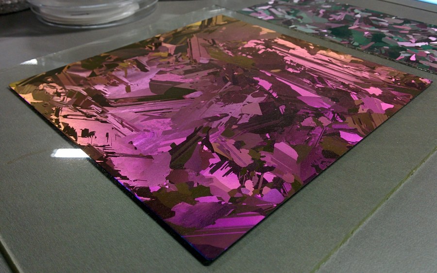
A bare multicrystalline wafer under an anti-reflective film. Every visible domain is a separate crystal grain, and every line between two domains is a boundary where the lattice breaks. Photo by Radiotrefoil, CC BY-SA 4.0.
A photon absorbed in silicon frees an electron and leaves a hole behind. That pair has to survive long enough to reach the junction and be collected. Anything that lets the two recombine on the way is a loss. Average survival time carries the name minority carrier lifetime. Grain boundaries attack that lifetime directly. Where two lattices meet at different orientations, bonds cannot line up. The mismatch leaves dangling bonds and dislocations behind. Those defects introduce extra energy levels inside the bandgap.
A carrier that would otherwise need a full 1.12 electronvolt jump can drop into one of those intermediate levels and recombine there. That makes a boundary a highly localised region of recombination. Two further effects come with the boundary. It blocks carrier flow across itself. Carriers generated in one grain struggle to reach a junction beyond it. It also provides shunting paths across the p-n junction. Some of the collected current leaks back there in place of leaving through the terminals.
Follow that through into the voltage equation and the connection becomes exact. Open-circuit voltage equals the thermal voltage multiplied by the natural log of the light-generated current divided by the saturation current. Recombination is what the saturation current measures. More recombination raises that current. The ratio inside the logarithm falls. A lower open-circuit voltage is where the cell settles. A multicrystalline cell gives up voltage for a mechanical reason: its lattice is interrupted. Impurities compound the effect. Grain boundaries act as collection sites, gathering metallic contamination and precipitates during the long cool-down after casting. Performance in cast material is limited mainly by recombination at dislocations and intragrain defects of exactly that kind.
The counterintuitive turn in grain size
Larger grains sound obviously better. Fewer boundaries per wafer means less boundary area for carriers to meet, and early cast material was pushed toward grains as large as the process could manage. Grain sizes on the order of at least a few millimetres are needed before boundary recombination stops dominating the result. Then the industry went the other way. High performance multicrystalline material, the last generation of the cast route, used seeded growth to produce grains deliberately smaller than the previous norm. Smaller grains create lower stress at the boundaries. A boundary under less stress carries fewer dislocations, which leaves it less electrically active. The lesson generalises past this one material. Boundary count was never the quantity that mattered. Boundary quality was. A wafer full of small, clean, low-stress boundaries can outperform one with a few large boundaries loaded with dislocations.
Dislocation clusters are the specific enemy that stress creates. A boundary between two grains at a large misorientation angle carries a dense array of them. Each dislocation is a line of broken bonds threading into the crystal. Impurities decorate those lines during cooling, which turns a geometric defect into an electrical one. Seeded growth attacks the problem at its origin by keeping misorientation angles small. That refinement bought the cast route several years of competitiveness. It never closed the gap. A single crystal has no boundaries at all. No boundary quality problem exists there to solve.
The efficiency numbers as they stand
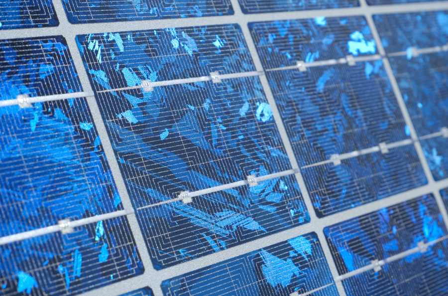
Polycrystalline cells at module scale. The cells are full squares with no chamfered corners, and the flecks are grains meeting the surface at different angles. Photo by Guilhem Vellut, CC BY 2.0.
Current polycrystalline modules deliver 15 to 17 percent efficiency. Monocrystalline modules in general production deliver 19 to 22 percent, with the best mass-produced lines quoted at 22 to 24. The gap at module level sits somewhere around four to six percentage points. Efficiency here means the fraction of incident light energy leaving as electricity, measured under 1,000 watts per square metre of test light. A 17 percent module receives 1,000 watts on each square metre and delivers 170. A 21 percent module delivers 210 from the identical square metre. Cell efficiency and module efficiency are separate measurements. The difference matters when comparing datasheets. A module includes the gaps between cells, the frame, the glass reflection and the resistance of every ribbon. Quoting a cell number where a module number belongs inflates the figure by several points. The substitution is common in this market.
Manufacturers track the shortfall as cell-to-module loss and spend real engineering on shrinking it. Gaps between cells, ribbon resistance, glass reflection and the frame all live in that number. Two modules built from identical cells can differ by a point of module efficiency on the strength of layout and interconnection alone, which is why cell efficiency makes a poor proxy for what a panel delivers. Record laboratory cells sit far above either production figure. Those records come from processes nobody runs at volume. They set a direction of travel. What arrives in a box is described by the production figures.
The square that is not quite square
Here the geometry pays part of the efficiency gap back, and almost nobody mentions it. A cast block is square. Wafers cut from it are full squares. They tile a module with no wasted corners. A pulled crystal is a cylinder. Wafers cut from it start round. Squaring a round wafer means cutting away the edges. Cutting all the way to a full square would waste enormous quantities of silicon. The industry settled on the pseudo-square: a square with four corners left rounded where the original cylinder ran out. That shape is why monocrystalline cells have chamfered corners and cast cells do not. Work out what the chamfers cost. A 125 millimetre pseudo-square cut from a 150 millimetre cylinder covers 14,858 square millimetres against 15,625 for a full square, which is 4.91 percent of the footprint given away. Move to a 156 millimetre cell from a 200 millimetre cylinder and the loss falls to 1.81 percent. Modern 166 millimetre cells from 223 millimetre cylinders give up 0.51 percent.
Those percentages are module-level figures. Sawing takes its own cut before any of that. Every wafer separated from a cylinder or a block leaves behind a slot of silicon turned to dust, and for decades that kerf loss ran comparable to the thickness of the wafer itself. Diamond wire sawing narrowed the slot and sped the cut, which lowered the silicon consumed per wafer across the industry. The change helped the pulled cylinder more, since a cylinder costs far more per kilogram than a cast block and every gram saved is worth more. A monocrystalline module carries slightly less active silicon per square metre of glass than a polycrystalline module of the identical dimensions, and part of the cell efficiency advantage is spent covering that. The effect was substantial on older small formats. It has nearly vanished on current large formats. The mono advantage reads larger today for that reason alone.
What four points of efficiency buys
Efficiency reaches a portable owner as area and weight. Take a hundred watt panel as the unit and work both cases at test conditions. A 17 percent module makes 170 watts from a square metre. One hundred watts needs 0.59 square metres of aperture. A 21 percent module makes 210 watts from a square metre. A hundred watts there needs 0.48. The difference is about 0.11 square metres, which on a folding panel is a whole extra panel section to carry, hinge and store. Weight follows area for framed modules, since glass and frame dominate the mass. A rigid hundred watt panel at 7.5 kilograms built on 17 percent cells would want roughly a fifth more glass area than one built on 21 percent cells. That is roughly 1.5 kilograms of extra glass and frame on a hundred watt module. Scale the comparison to a machine worth filling and the area difference stops being academic. Four hundred watts of panel at 21 percent covers 1.9 square metres. The identical 400 watts at 17 percent covers 2.35. Those extra 0.45 square metres amount to another folding section, another hinge, another kilogram. The case stops closing on the back seat. Fixed installations absorb the difference by using more roof. Anything carried absorbs it by getting heavier. Mounting hardware scales with area as well. A larger panel needs a longer stand, a wider bracket, more roof rail. It also presents more sail area to wind. Portable owners meet that as a folding case that no longer fits behind a seat. Fixed installations meet it as a rack bill. Energy per day scales with nothing except rated power, which is the part people get wrong. Two hundred watt panels of different efficiencies produce the identical energy under the identical sun, because both are rated at a hundred watts. Efficiency decides how much surface those hundred watts required, never how many watt-hours they deliver.
Heat, dim light, and the flaw that was mono alone
Temperature coefficients differ between the two materials by less than most comparisons imply. Published averages put monocrystalline at about minus 0.38 percent per degree and polycrystalline at about minus 0.40. Run that over a 40 degree rise above test conditions and the difference amounts to 0.8 percent of rated power. Cell architecture moves that number far more than crystal structure does. Monocrystalline n-type back-contact cells reach about minus 0.30 percent per degree. Heterojunction cells reach about minus 0.25. Those are differences of 0.10 to 0.15 percent per degree against the mono average, several times the gap between mono and poly. Low light behaviour follows a similar pattern. Both materials produce current in near proportion to irradiance. Both hold voltage reasonably well as light falls. Claims that one chemistry dramatically outperforms the other under cloud rarely survive a measurement. Low light response is set by shunt resistance and junction quality, with grain structure a long way down the list.
One weakness belonged to the pulled crystal alone. Closing it took the industry twenty years. A Czochralski melt sits in a quartz crucible. Quartz is silicon dioxide. The growing crystal takes up interstitial oxygen from its own container. Industrial Czochralski silicon carries significant quantities of it. Where the wafer is also doped with boron, light exposure drives boron and two oxygen atoms into a complex. That complex acts as a recombination centre, and output falls in the first hours of sunlight.
The literature calls it the boron-oxygen complex. It is the dominant light-induced degradation mechanism in this material. Cast silicon carried far less of that burden. A graphite-lined crucible and a faster process leave less dissolved oxygen behind. For a while that was a genuine advantage held by the cheaper material. The fix arrived in the dopant, leaving the crucible alone. Replace boron with gallium and the complex has no boron to form from. Gallium-doped Czochralski silicon is immune to that degradation mode. The industry moved across.
Appearance is the one place the difference is unmistakable. Monocrystalline cells look uniformly dark because a single lattice presents one orientation to the light. Polycrystalline cells look flecked and blue because each grain meets the surface at its own angle and scatters differently. A buyer can identify the material across a car park, with no datasheet in hand and no meter.
Why one of them disappeared
Cast silicon existed for one reason: cost per watt. The process was cheaper per kilogram of usable wafer, and for two decades that saving outweighed the efficiency it gave up. Three changes removed the saving. Diamond wire sawing replaced slurry sawing and cut kerf loss for every wafer, which helped the pulled cylinder more than the cast block. Crystal pullers grew larger and ran longer, spreading the fixed cost of a pull across far more wafers. Cell architectures that reward good material, PERC among them, arrived and returned more efficiency on a single crystal than on a cast one. The third of those deserves unpacking. It explains why the gap widened. A passivated emitter and rear cell adds a dielectric layer across the back surface to stop carriers recombining there. That improvement only pays when rear recombination is what limits the cell. In cast material the bulk already dominates, because carriers meet a grain boundary long before they reach the back face. Passivating the rear of a wafer whose interior is the problem returns very little. Applying it to a single crystal, where the bulk is quiet, returns a great deal. Every architecture that rewards good material behaves that way. Each generation of cell design pushed the two further apart.
Cost per watt is where the decision actually got made. The arithmetic is short. Divide the price of a finished wafer by the watts that wafer becomes. A mono wafer costing 15 percent more than a cast one, yielding 25 percent more watts, is already cheaper per watt. Every reduction in pulling cost moved that ratio one way. Cast silicon lost its advantage without ever getting more expensive. Market figures record the outcome. Monocrystalline products hold the dominant share of the photovoltaic wafer market and continue to grow, with PERC alone accounting for close to half the technology segment. Polycrystalline panels are now described in the trade as largely obsolete. Two practical consequences follow for a buyer. New polycrystalline panels in the portable class are increasingly hard to find at any price. Second-hand and old-stock polycrystalline panels are cheap. For a fixed installation with space to spare they remain serviceable hardware.
Monocrystalline against polycrystalline, by the figures that differ
Quantity
Monocrystalline
Polycrystalline
How the silicon solidifies
pulled from a seed, one continuous crystal
cast and cooled from below, many grains
Module efficiency
19 to 22 percent, best lines 22 to 24
15 to 17 percent
Area needed for 100 W
0.48 m² at 21 percent
0.59 m² at 17 percent
Wafer shape
pseudo-square, corners chamfered
full square
Footprint lost to chamfers
4.91 percent at 125 mm, 0.51 percent at 166 mm
none
Temperature coefficient of power
about -0.38 %/°C
about -0.40 %/°C
Grain boundaries
none inside the wafer
millimetre-scale grains throughout
Appearance
uniform dark surface
flecked blue surface
Market position
dominant and growing
largely obsolete
Buying a portable panel today
Anyone shopping for a folding panel will find monocrystalline on nearly every listing. The supply chain has already made that choice. What remains is checking the stated efficiency against the stated size.
Check the claim against the physical size. Divide rated watts by the unfolded area in square metres, then divide by 1,000 to get module efficiency as a fraction. A hundred watt panel measuring 1.13 by 0.595 metres covers 0.672 square metres and works out at 14.9 percent. That is a polycrystalline-class number on a listing that says monocrystalline.
Two innocent explanations exist for a gap like that. The quoted dimensions may include the fabric border and the stitching, which carry no cells. The rating may be a peak figure measured somewhere other than Standard Test Conditions. Both deserve a question to the seller.
Second-hand stock is where most people will meet cast silicon now. Panels pulled from ten and fifteen year old roof arrays reach the market in quantity, typically 240 to 280 watts in a frame close to 1.65 by 1.0 metres. Those are excellent value for a shed, a workshop or a fixed off-grid rack. They weigh 18 to 20 kilograms each, need real mounting hardware, and present an open-circuit voltage in the high thirties that most portable machines will refuse. Buying one to feed a power station is a common and expensive mistake. Check the plate against the machine before the money moves. Comparing one panel with another panel answers a different question. Any open-circuit figure above the machine’s stated input ceiling rules the panel out, whatever its price per watt says.
Where a genuine polycrystalline panel turns up cheaply, weigh area against price. For a roof, a shed or a boat with room to spare, cast silicon at half the price per watt does the identical job with more surface. For anything carried, the extra 0.11 square metres per hundred watts eventually decides the matter.
Common questions
Do monocrystalline panels produce more power than polycrystalline ones?
Not for a given rating. A hundred watt panel of either material produces a hundred watts under test light. Monocrystalline reaches that rating in less area. Efficiency describes exactly that.
Why do polycrystalline cells look blue and flecked?
Each grain meets the surface with its own crystal orientation. The anti-reflective coating and the texture behave slightly differently on each one. The eye sees that as flecks. A single crystal presents one orientation everywhere and looks uniform.
Is polycrystalline worse in hot weather?
By a small margin. The published averages are about minus 0.40 percent per degree against minus 0.38 for monocrystalline, which comes to under one percent of rated power at 40 degrees above test conditions. Cell architecture matters several times more.
Should I replace working polycrystalline panels with monocrystalline ones?
Only where area is the constraint. A working panel producing what it always produced owes nobody an upgrade. Embodied energy in a replacement takes years to earn back.
Why are the corners of monocrystalline cells cut off?
Because the wafer began as a slice of a cylinder. Squaring it completely would throw away a large fraction of an expensive crystal. The corners stay rounded where the cylinder ended. Cast wafers come from a square block and need no such compromise.