Wide-Bandgap Power
Weighing SiC Against GaN
Silicon carbide and gallium nitride are wide-bandgap semiconductors, materials whose wider energy gap lets a transistor hold off more voltage in less material, switch faster, and run hotter than a silicon part of the same rating. The two have split the ground silicon handled poorly: silicon carbide carries the high-voltage, high-power loads, and gallium nitride takes the lower-voltage, high-frequency ones. Weighing them is a matter of reading the voltage, the frequency, and the power a design needs, then choosing the material that fits that corner and the part and gate drive that go with it.
What wide-bandgap buys
The wider gap raises the field the material withstands before it breaks down, so a wide-bandgap device blocks a given voltage in a thinner, lower-resistance layer than silicon needs. That cuts the conduction loss and the switching loss at once, so a converter built on these parts runs at a higher frequency and a higher efficiency than a silicon design, and the smaller magnetics and the lighter cooling follow from it. The higher frequency is the lever, since the inductor and the transformer shrink as the frequency climbs, so a wide-bandgap supply can be a fraction of the size and weight of the silicon one it replaces. The gain comes from the material, so it shows up across the whole design, in the heatsink, the magnetics, and the energy bill alike.
The saving is not free at the counter. Working out the total cost of ownership for SiC against silicon MOSFETs is how the case gets made, since the wide-bandgap die costs more than the silicon it replaces, and the payback shows up in a smaller inductor, less heatsink, and the energy saved over the life of the product. On a high-power supply that runs for years, the lower loss covers the higher part price; on a low-duty board it may not. The system saving is where the real case lives, since a design that drops a fan, shrinks a heatsink, and uses a smaller transformer can come out cheaper at the system level even with a costlier switch. The calculation is run for the specific duty cycle and the energy price the product sees, not assumed from the datasheet efficiency alone.
The two materials divide the work by voltage and frequency.
Picking the side of the line a design sits on, the work of choosing between GaN and SiC by voltage and frequency, comes down to a few rules: gallium nitride owns the band up to about 650 volts where its speed shrinks the supply, silicon carbide owns the high-voltage classes from 650 volts to well past a kilovolt, and in the overlap the frequency and the power decide which one wins. At 650 volts both materials compete, so a high-frequency, lower-power stage there leans toward GaN and a high-power one toward SiC, and the design reads its own numbers for the stage at hand, since a blanket rule misses the case at the boundary.
The SiC parts
Silicon carbide has several established suppliers, and the choice often starts with availability. The lead time and pricing on Wolfspeed SiC MOSFETs shape many designs, since the company is one of the largest SiC makers and its delivery sets the schedule, and the Infineon CoolSiC reliability positioning markets a part qualified for the long field life an industrial or automotive design demands.
The device generations move quickly. Comparing the ROHM SiC Gen 4 against Gen 3 is a generation question, since each step cuts the on-resistance for the same die area and trims the switching loss, so a new design starts from the current generation and an existing one moves when the gain pays for the requalification.
The package follows the power level. Knowing where ON Semi SiC modules fit covers the high-current stages that need the dies and the thermal base in one housing, and sourcing the ST 1200V SiC MOSFETs covers the discrete parts for the 1200-volt class that a solar string or an industrial drive runs at. The 1200-volt class is the workhorse rating for SiC, since it covers the 800-volt automotive bus and the three-phase industrial rails with margin, so a large share of the SiC catalog sits there and the sourcing choice is broad.
The body diode is a SiC detail of its own. A SiC MOSFET carries an intrinsic body diode with a higher forward drop than a silicon part, so a synchronous design turns the channel on to carry the reverse current and spares that drop, and a part chosen for a hard-switched bridge is read on its body-diode behaviour alongside its on-resistance.
The supply base has widened. Assessing the production readiness of Chinese SiC MOSFETs has become part of a cost-down review, once the part is checked on its on-resistance, its gate-drive window, and its switching ruggedness against the established makers.
The GaN parts
Gallium nitride sits at the lower voltages and the highest frequencies, and its parts come from a younger set of makers. Using the GaN Systems 650V GaN for grid-tied products covers the half-bridge parts that a solar microinverter or an on-grid converter runs at the top of the GaN voltage range, where the fast switching cuts the magnetics and the loss. A GaN HEMT is a lateral device with no intrinsic body diode, so it has no reverse-recovery charge to clear, which is a large part of why it switches cleaner and faster than a silicon part at these voltages. The device conducts in reverse through its channel, so the dead-time behaviour is designed around that conduction and not around a diode recovery.
The low-voltage end is its own field. Knowing where EPC low-voltage eGaN fits covers the parts below a hundred volts for a high-density DC-DC converter, a class-D amplifier, or a lidar driver, where the tiny gate charge and the absence of reverse recovery let the stage switch at a speed silicon could not reach.
GaN brings a packaging answer of its own. The Navitas GaNFast integrated driver value is in putting the GaN switch, its gate driver, and its protection in one part, since GaN switches so fast that a separate driver and a stray loop throw away the speed, and integrating the driver onto the device holds the loop tight and makes the part usable without a specialist gate design. The integration also adds the protection a bare GaN device lacks, since the part has little tolerance for overcurrent or overvoltage, so a monolithic driver brings the sensing and the shutdown that keep it inside its narrow safe area. For a team without deep wide-bandgap experience, that integration is the difference between a part it can design in and one it cannot.
Designing them in
The gate drive is where a wide-bandgap design is won or lost. The negative-voltage rule for SiC MOSFET gate drive is the first thing to get right, since a SiC MOSFET has a low gate threshold and a narrow drive window, so the gate is pulled to a negative voltage at turn-off to hold the device firmly off against the fast voltage steps a bridge throws at it, and the positive drive is held within the tight range the datasheet allows. Overdrive the gate past that range and the device degrades; underdrive it and the on-resistance rises and the part runs hot, so the SiC gate supply is regulated more tightly than a silicon design needs. GaN is tighter still, since a GaN HEMT tolerates only a narrow gate voltage above its threshold, so its driver is built for that part and rarely shared with a silicon design.
The application pulls the material along with it. The move to SiC in automotive onboard chargers is one of the clearest cases, since the onboard charger and the traction inverter of an electric car run at high voltage and high power where the SiC efficiency cuts the heat, the weight, and the charging time, and the higher part cost rides on a vehicle that can carry it. The 800-volt battery architectures now reaching production lean on SiC directly, since silicon struggles at that bus voltage and SiC handles it with margin, so the move up in battery voltage pulls SiC along with it. The reliability qualification an automotive part carries is part of the cost, which is why the established SiC makers lead in that market.
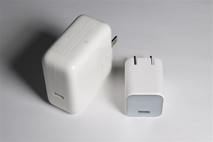
The consumer end went the other way. The reason 65W fast chargers moved to GaN is that the high switching frequency shrinks the transformer and the capacitors, so a GaN charger fits a fraction of the size of its silicon predecessor, and the volume of the phone-charger market drove the GaN price down to where it pays. That volume is what tipped GaN from a costly specialty into a mainstream part, since the charger market buys in the hundreds of millions and pulled the price down for every other GaN design along the way. A 65-watt charger the size of a wall plug is the visible result, and the same parts now reach into adapters, lighting, and small converters.
How wide-bandgap parts get chosen and sourced
A wide-bandgap part is specified as a device, a gate-drive scheme, and a thermal and layout design together, so a substitution that keeps the voltage and current can still fail if its gate-drive window, its switching speed, or its package parasitics differ. A broad-line distributor that carries the SiC and GaN families across the voltage classes and the major makers lets a design source the device and a checked equivalent, and weigh the lead time that a fast-growing supply base still carries. The SiC supply has tightened in waves as automotive demand has grown, so a design that leans on a single SiC part watches its lead time as closely as its price, and qualifies a second source where it can. The GaN supply is younger and more concentrated, so a part is checked for a second maker before a design commits to it. The voltage and frequency the design runs are the constants the selection answers to, since they fix the material before the vendor and the package come into it.
The judgment that fits
Read the voltage, the frequency, and the power: take silicon carbide for the high-voltage, high-power stages and gallium nitride for the lower-voltage, high-frequency ones, design the gate drive the material demands, and check that the efficiency saved pays back the part.
The fourteen pages below take the SiC makers, the GaN makers, and the design and cost questions one at a time.