MOSFET Selection
MOSFETs by Conduction Loss and Thermal Budget
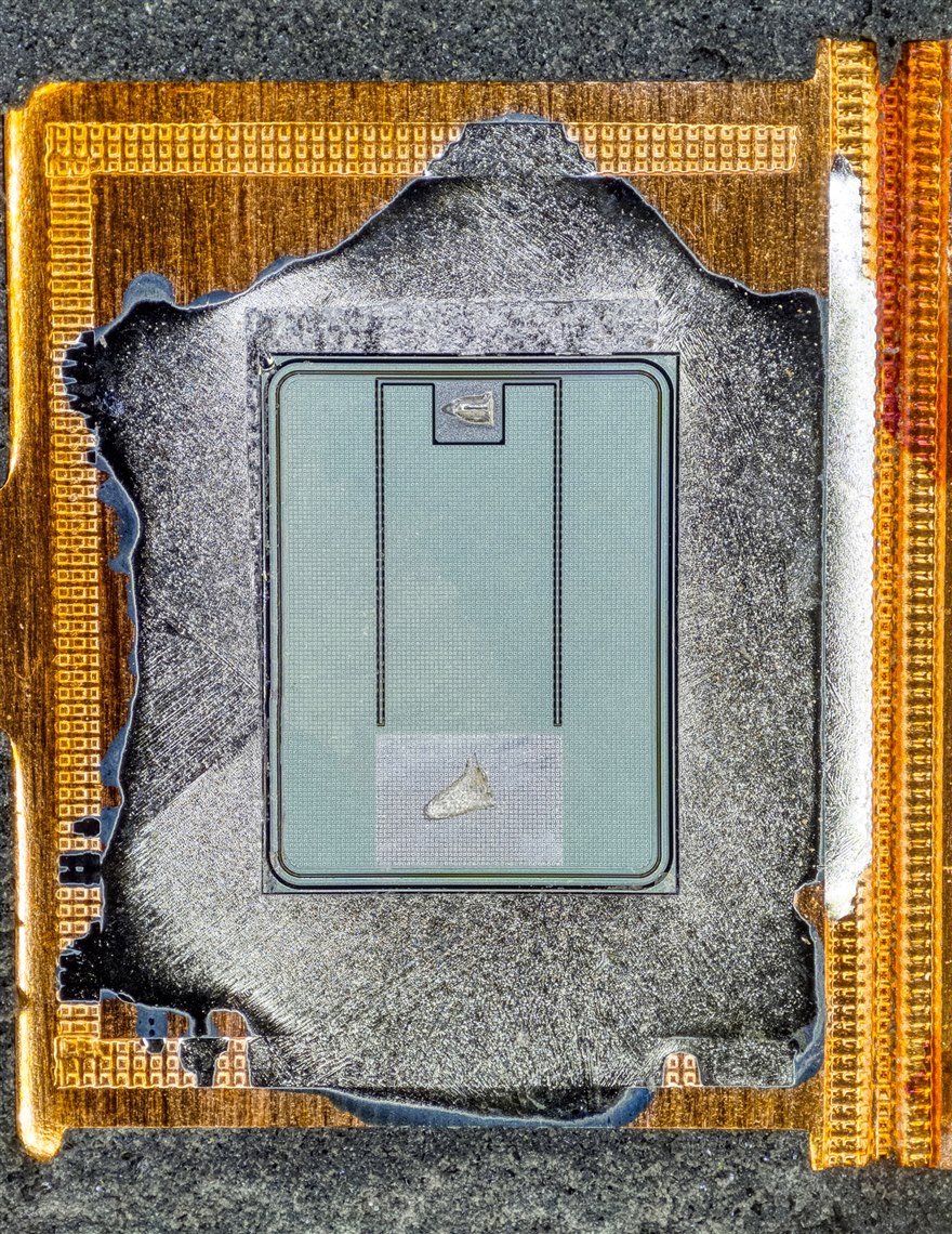
A power MOSFET is the voltage-controlled switch that carries the current in the great majority of low and middle-voltage supplies, motor drives, and load switches, and choosing one is a matter of keeping its losses inside the heat the board can shed. The part makes two kinds of loss: conduction loss as it carries current through its on-resistance, and switching loss each time it turns on and off. Both end up as heat in the junction, so the selection works from the thermal budget back to a part whose on-resistance, gate charge, and package keep that junction cool at the current and frequency the design runs. A part that looks ideal on its on-resistance can still be the wrong choice once its gate charge and its package thermals are read against the job, which is why the selection is a balance of three or four numbers weighed together at the operating point.
The parameters that set the losses
On-resistance is the number a MOSFET is known by, since it sets the conduction loss directly. How on-resistance drives conduction loss is the first thing to read, because the loss is the current squared times that resistance, so a part with half the on-resistance burns half the conduction heat at the same current. The figure climbs with temperature, so the value at a hot junction matters more than the cool-bench number on the front of the datasheet. On-resistance roughly doubles from room temperature to a junction near its limit, so a part picked on its 25-degree number can run far hotter than the sum suggested once the board warms up, and the honest calculation uses the resistance at the temperature the part will sit at.
Gate charge sets the other half. How gate charge sets switching speed decides the switching loss, since the gate driver has to move that charge in and out every cycle, and a part with a large gate charge switches slowly and burns more energy in each transition. A low on-resistance often comes with a large gate charge on the same process, so the two are read together at the frequency the design runs, and the best part for a slow load switch is the wrong one for a fast converter. The figure of merit a vendor quotes, the product of on-resistance and gate charge, captures this balance in one number, and it is the honest way to compare two parts aimed at switching duty. At a few hundred kilohertz the gate charge starts to dominate the loss, so a converter designer reads that product before the headline on-resistance, and a load switch that turns on once a second ignores the gate charge and chases the lowest resistance it can buy.
The body diode is the part designers forget.
Every MOSFET carries a diode across its drain and source, and in a synchronous converter that diode conducts during the dead time and then has to recover. The behaviour of body diode recovery in synchronous rectification adds loss and a current spike each cycle, so a part for the high side of a synchronous buck is chosen on its recovery charge as much as its on-resistance. A soft, slow body diode that recovers poorly can spike the switching node and stress the opposite switch, which is the failure that turns a converter that passed at low load into one that fails hot at full load.
Two more ratings decide whether a part survives its worst moment. What the avalanche rating means in selection covers the energy the part can absorb when an inductive load drives it past its breakdown voltage, the event that kills an underrated switch in a motor or a solenoid drive. And how junction temperature sets lifetime ties the whole selection back to heat, since the part ages faster the hotter it runs and the margin below its rated junction is bought on purpose. Thermal cycling does its own damage, since each warm-up and cool-down works the solder joints and the die attach, so a part that swings through a wide temperature range every cycle wears out sooner than its steady-state rating alone would predict. The rated maximum junction temperature is a limit, not an operating point, and a design that lives near it trades its service life for the few cents a smaller part saved.
Driving and placing the part
A MOSFET only delivers its datasheet on-resistance once its gate is driven hard enough. Setting the gate drive voltage is the step that turns the part fully on, since a gate driven to a voltage between the threshold and the rated level leaves the channel half-enhanced and burning extra heat, and a logic-level part is chosen when the controller or the gate driver cannot swing the standard 10 V that a classic MOSFET wants to turn on fully.
The high side asks for more than a part swap. Knowing why high-side switching is not just a P-channel covers the gate-reference problem, since an N-channel high-side switch needs its gate driven above the supply with a bootstrap or a charge pump, and reaching for a P-channel to dodge that brings its own higher on-resistance and cost. The drive scheme is part of the device choice, settled alongside the part.
Layout finishes what the device starts. A MOSFET switching fast throws current edges into the loop around it, so a long trace to the gate driver or a loose power loop turns into ringing, extra loss, and radiated noise that the rest of the board has to live with. The gate resistor sets how fast the edge moves, trading switching loss against that overshoot, so the part is placed close to its driver and its decoupling and the loop is kept tight before the speed on the datasheet shows up on the bench.
The parts that fill the sockets
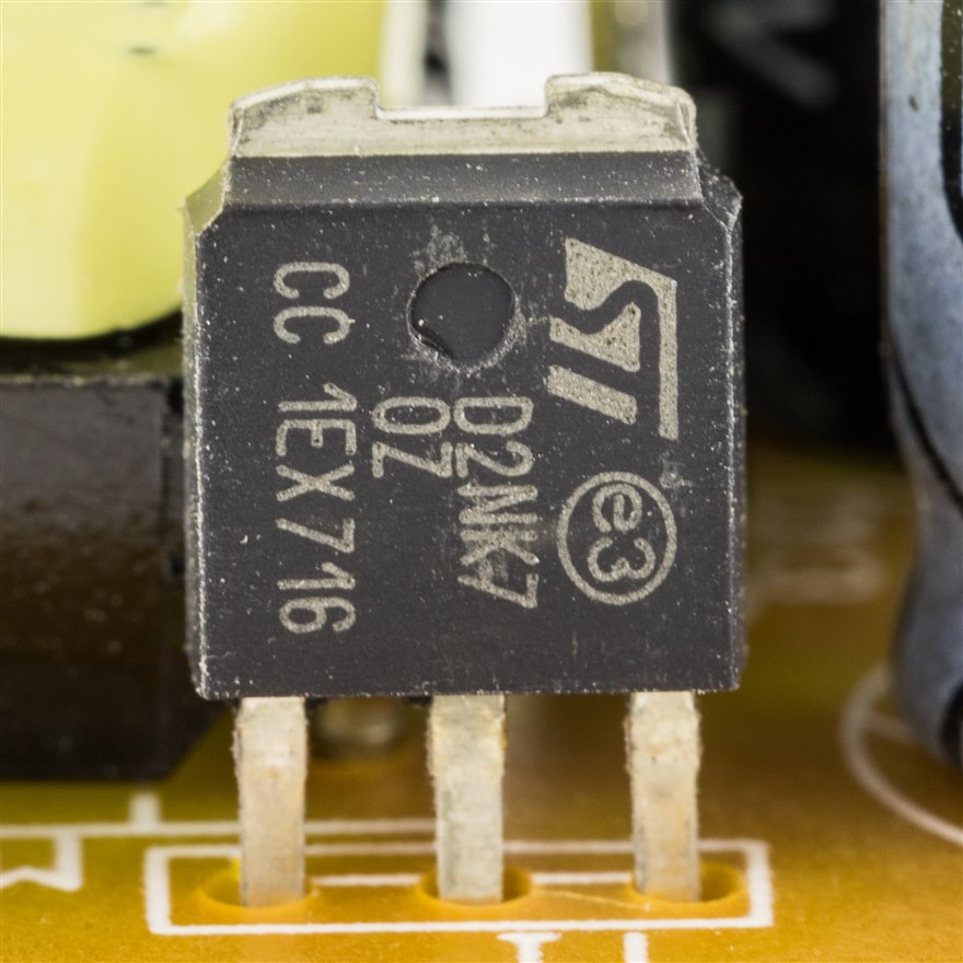
The catalog sorts first by voltage class, since a part is rated for a maximum drain-source voltage and a design picks one with margin above the rail it switches plus the spikes the layout throws at it. A 30 V part suits a single-cell or a 12 V rail, a 100 V part a 48 V bus, and reaching for more voltage than the job needs costs on-resistance for nothing. Within a class the choice runs by vendor and grade. For the high-performance trench parts, selecting from the Infineon OptiMOS line covers the low-voltage, low-on-resistance sockets a synchronous converter needs, and the Toshiba U-MOS VIII price premium buys a similar grade where the figure of merit earns its keep. For dense boards, the Vishay Si4 PowerPAK MOSFET applications cover the power-density sockets where the package thermal path matters as much as the die. The package is half the thermal story on a surface-mount part, since a die with a low on-resistance does no good if the package and the board cannot pull its heat out, so a power-density design reads the junction-to-board thermal resistance and the copper it assumes alongside the silicon spec.
Cost and availability drive a large share of the choices. The value case for Nexperia low-voltage MOSFETs is the price-per-amp on a high-volume board, and the availability of ON Semi general N-channel MOSFETs keeps a design fed with a jellybean part that is always in stock. Where the budget pushes hardest, the maturity of Chinese MOSFETs as Infineon replacements has reached the point a cost-down review takes seriously, once the part is checked on its real on-resistance and avalanche numbers. The gap that remains is in the datasheet detail and the long-term supply record, so a Chinese part with a solid avalanche spec and a credible production history earns a slot on a cost-driven board, and one with a thin datasheet stays off a design that has to ship for years.
Old designs carry old parts. Many boards still specify the IRFZ44 or the IRF540, and moving off the IRFZ44 and IRF540 to modern MOSFETs cuts the on-resistance several times over and the gate charge with it, which a refresh of an aging product pays back in heat and efficiency. The footprint often carries across, so the swap can be a drop-in on the board even as the gate drive and the thermal numbers improve, and a redesign for any other reason is the moment to retire the decades-old part.
One job has its own rules. The selection of battery-protection MOSFETs turns on a low on-resistance at a low gate voltage and a back-to-back pair that blocks current in both directions, a niche a general switch does not fill. The pair shares one package so the two dies sit at the same temperature, and the gate threshold is set low so a nearly flat lithium cell can still drive them fully on, which is the corner that rules out a part designed for a 10 V gate.
How MOSFETs get chosen and sourced
A MOSFET is read on a chain of numbers that ends at junction temperature, so the part, its drive, and the board’s cooling are specified together, and a substitution that keeps the voltage and current ratings can still run hot if its on-resistance, its gate charge, or its thermal resistance differ. A broad-line distributor that carries the MOSFET families across the voltage classes and the major vendors lets a design source the switch and a checked equivalent in the same package, which keeps a power stage off a single source when a popular part goes on allocation. The thermal budget is the constant the selection answers to, since the same die runs cool on a board with copper to spare and burns up on a cramped one. A second source matters more on a MOSFET than on many parts, since a swap is read on on-resistance, gate charge, avalanche energy, and the package thermal path together, and a part that matches the headline voltage and current can still differ on the numbers that set the heat. Pinning down a checked equivalent early keeps a power stage from a redesign when the first-choice part goes long on lead time.
The judgment that fits
Read the on-resistance and the gate charge at the temperature and frequency the design runs, give the part a gate drive that turns it fully on, and leave junction-temperature margin below the rating. The fifteen pages below take the parameters and the parts one at a time, from on-resistance and gate charge through the vendor families and the parts a battery or a high-side socket calls for.